This thread has been locked.

If you have a related question, please click the "Ask a related question" button in the top right corner. The newly created question will be automatically linked to this question.

[FAQ] 关于boot的总结

Other Parts Discussed in Thread: CCSTUDIO, OMAP-L138, SYSBIOS

本人总结了关于TI DSP的boot原理,格式,以及参考代码供大家参考。不足之处,敬请指正。

2014.12.8: 更新:改成CCSV5.5工程,内容稍做修改与简化。

也可以参考Starterware里的bootloader example,说明如下:

C6748 StarterWare Booting And Flashing

Contents

The StarterWare Bootloader[edit]

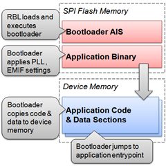
The StarterWare bootloader is a platform-specific helper application that makes it easy to transition from running a StarterWare application in a debug context (i.e. in Code Composer Studio with a GEL file) to a production context (i.e. running the application automatically when the board is powered on). The bootloader acts as an intermediary between the ROM bootloader (RBL) and the application. During boot, the StarterWare bootloader takes the following actions:

  1. Applies common PLL and DDR/EMIF settings
  2. Copies application program and data sections from flash memory to DDR
  3. Jumps to application entrypoint

If the bootloader encounters an error during boot, it prints diagnostic messages to the UART console.

The StarterWare bootloader comes pre-built with the standard installation and typically does not need to be modified or rebuilt unless you want to port it to a custom hardware platform. The prebuilt binary can be found in the following location:

<StarterWare Installation Path>/binary/armv5/<toolchain>/c6748/evmC6748/bootloader/Release/boot.out

Booting a StarterWare Application[edit]

Binary Image Generation[edit]

Booting a StarterWare application requires two binary images:

  1. An AIS file containing the StarterWare bootloader
  2. A binary file containing the application

These images are generated using two separate tools, both of which are included in the tools folder of the standard StarterWare installation.

Using AISgen to Create the Bootloader AIS File[edit]

The AISgen GUI can be used to generate the StarterWare bootloader AIS file. All of the critical settings are located on the General tab of the AISgen GUI:

  • Boot Mode - Set to SPI0 Flash
  • Application File - Set to bootloader .out file
  • AIS Output File - Desired AIS file name/path

The AISgen tool has many options to configure the device at boot time, but these are generally not necessary since the StarterWare bootloader will boot very quickly and apply its own configuration immediately. The following screenshot shows the typical settings that should be specified to generate the bootloader AIS file. Simply click the Generate AIS button to create the AIS file.

NOTE
You will typically need to generate the bootloader AIS file only once. That same AIS file can be used with any number of different applications.

Using out2rprc to Create the Application Binary[edit]

The out2rprc command line utility is used to generate the application binary image. This tool strips out the initialized sections from the executable file (i.e. *.out) and places them in a compact format that the StarterWare bootloader can understand. Generating this binary file is very simple:

$> out2rprc.exe [application].out [application].bin

The output (bin) file is typically much smaller than the original executable (out) file.

Flashing the Application[edit]

Once you have generated both binary images (i.e. the AIS and bin files described above), you are ready to flash these images to the EVM's SPI flash memory. This can be done using the standard serial flasher utility that's included in the tools folder of the standard StarterWare installation:

  1. Set the boot switches for UART2 boot (5:8 = 0011 on EVM)
  2. Run SFH from the command line:
    • $> sfh_OMAP-L138.exe -flash -targetType C6748 [bootloader].ais [application].bin
  3. Power on or reset the EVM

The SFH tool may take several minutes to complete depending on the size of the application. When SFH completes successfully, your application is ready to boot.

NOTE
The SFH tool automatically adds simple header information to the application binary file. This header tells the bootloader basic information about the application contents, including its total size in bytes.

Booting the Application[edit]

After the binary images have been flashed to the EVM, the application is ready to boot. This is as simple as setting the boot switches for SPI0 flash boot (5:8 = 0000 on the EVM) and powering on or resetting the board.

During boot, control passes from the ROM bootloader to the StarterWare bootloader, which configures the system and loads the application. Finally, the bootloader jumps to the application entrypoint. The overall process is summarized in the following diagram.

Boot_DSP_on_SOC_V0.2.zip
  • Hi  Tony,不好意思,有个boot的新问题:

    连仿真器后先load load原始的OMAPL138DemoInterrupt.out文件通过CCS run,LED如预期闪烁。

    然后我通过自己写的UBL程序将OMAPL138DemoInterrupt的二进制代码烧进FLASH后再读出来运行失败(LED没动静),load symbols也停不到任何代码行处。

    不断开仿真器再load原始的OMAPL138DemoInterrupt.out文件,单步运行发现会在_call_swi(327680);处跑飞再也执行不下去——

    为什么会这样?

    断点重连仿真器后先操作原始工程又OK,接着弄UBL后又跑飞。

  • _call_swi(327680);

    这个函数是进入SWI模式,传递的参数是327680,这个参数没有特殊的意义,仅仅是自己定义用来在SWI ISR区分想要进入的处理分支。

    调用这个函数出问题,在于你的程序里有没有SWI exception的处理代码实现。

  • Jingang Yang 

    Jingang Yang 说:
    单步运行发现会在_call_swi(327680);处跑飞再也执行不下去

    对了,看一下这篇贴子的总结:

    http://www.deyisupport.com/question_answer/dsp_arm/omap_l1x/f/54/t/103692.aspx

  • Tony, 关于327680这个数值的意义我已了解,但我不解的是,我用的是你附件里的例程,按理说你例程里SWI的SWI Handler是有的——在handler.asm中。

    为什么这个工程单独下载.out运行OK,但转成.hex后再加载出来跳转后就不行了呢?

    我UBL工程中还把你那三个.asm文件都加进去了试了,也不行

  • Jingang Yang 说:
    然后我通过自己写的UBL程序将OMAPL138DemoInterrupt的二进制代码烧进FLASH后再读出来运行失败(LED没动静),load symbols也停不到任何代码行处。

    OMAPL138DemoInterrupt的二进制代码是如何转换而来的?

    Jingang Yang 说:
    单步运行发现会在_call_swi(327680);处跑飞再也执行不下去——

    这时是否跳到预期的SWI exception处并进入SWI exception handler?

  • 1、二进制代码由armhex.exe转换而来:CCSv**\tools\compiler\ti-cgt-arm_****\bin\armhex;

    2、PC到达_call_swi(327680)后F5(step into)就飞掉了

  •  进一步补充三个工程的信息:

    1、OMAPL138DemoInterrupt工程:就是本帖一楼的附件Boot_DSP_on_SOC_V0.2.zip中的那个,稍微改造了一下GPIO初始化和while(1)进行LED闪烁toggle。

    2、NANDWriter_ARM工程:通过\OMAP-L138_FlashAndBootUtils_2_40\OMAP-L138\CCS\NANDWriter这个工程改造了一下——DEVICE_init()之后不是nandwriter()而是自己写的read nand的一个函数,fopen读取armhex转换OMAPL138DemoInterrupt.out得到的OMAPL138DemoInterrupt.hex;然后再通过格式解析将各section数据载入对相应地址中;最后Entry切换至OMAPL138DemoInterrupt得到与1一样的LED闪烁效果。

    3、UBL_NAND工程:通过\OMAP-L138_FlashAndBootUtils_2_40\OMAP-L138\CCS\UBL_ARM改造而来,DEVICE_init()后有UART_open(),NAND_open(),然后读取写入到NAND中的OMAPL138DemoInterrupt.hex(与2中fopen的hex内容相同,通过beyondCompare确认),然后再通过相同方法进行格式解析将各section数据载入对相应地址中;最后Entry切换至OMAPL138DemoInterrupt,到_call_swi()处跑飞——后试过将这行代码注释掉再生成新的hex、烧写、读取、加载、运行,可以正常运行在while(1),但是LED却不闪烁……进一步分析工作:

    1)通过registers可以看到GPIO0ARM的OUT_DATA**确认GPxPy是有变化的;

    2)直接memory确认PSC的MDSTAT对应的GPIO寄存器值为0x00001E03——也是OK的(1、2两个工程也是这个值);

    彻底懵圈了……

  • 附上第三个工程的程序入口代码:


    // Boot entry point to setup the C environment
    #if defined(__TMS470__)
      #pragma TASK(boot);
      #pragma NO_HOOKS(boot);
      #pragma CODE_SECTION(boot,".boot");
    #endif
    void boot(void)
    {
      asm(" .global STACK_START");
      asm(" .global _stack");
      asm(" .global main");
      asm(" NOP");
      asm(" MRS r0, cpsr");
      asm(" BIC r0, r0, #0x1F"); // CLEAR MODES
      asm(" ORR r0, r0, #0x13"); // SET SUPERVISOR mode
      asm(" ORR r0, r0, #0xC0"); // Disable FIQ and IRQ
      asm(" MSR cpsr, r0");
      asm(" NOP");

      // Set the IVT to low memory, leave MMU & caches disabled
      asm(" MRC p15,#0,r0,c1,c0,#0");
      asm(" BIC r0,r0,#0x00002300");
      asm(" BIC r0,r0,#0x00000087");
      asm(" ORR r0,r0,#0x00000002");
      asm(" ORR r0,r0,#0x00001000");
      asm(" MCR p15,#0,r0,c1,c0,#0");
      asm(" NOP");

      // Setup the stack pointer
      asm(" LDR sp,_stack");
      asm(" SUB sp,sp,#4");
      asm(" BIC sp, sp, #7");

      // Call to main entry point
      main();

      asm("_stack:");
      asm(" .word STACK_START");
    }

    汇编比较弱,分析不出个子丑寅卯来,只能从注释里大概看出来做了些啥工作。

    第一个工程的程序入口代码:

    _init_stack:.asmfunc
      ; SET TO SVC MODE
      MRS R0, CPSR
      BIC R0, R0, #0x1F
      ORR R0, R0, #0x13
      MSR CPSR_CF, R0

      ; INITIALIZE THE SVC MODE STACK
      LDR SP, c_svc_stack
      LDR R0, c_SVC_STACK_SIZE
      ADD SP, SP, R0

      ; SET TO IRQ MODE
      MRS R0, CPSR
      BIC R0, R0, #0x1F
      ORR R0, R0, #0x12
      MSR CPSR_CF, R0

      ; INITIALIZE THE IRQ MODE STACK
      LDR SP, c_irq_stack
      LDR R0, c_IRQ_STACK_SIZE
      ADD SP, SP, R0

      ; SET TO FIQ MODE
      MRS R0, CPSR
      BIC R0, R0, #0x1F
      ORR R0, R0, #0x11
      MSR CPSR_CF, R0

      ; INITIALIZE THE FIQ MODE STACK
      LDR SP, c_fiq_stack
      LDR R0, c_FIQ_STACK_SIZE
      ADD SP, SP, R0

      ; Continue to _c_int00
      LDR PC, c_int00
      .endasmfunc

  • 你是说下面boot是你的工程的入口?这显然不对吧。要么你把工程一的这部分copy到你工程里来,一般都不自己写这部分,除非自己对写汇编有信心,还有对ARM的模式切换操作很熟。

    还有上面你说的飞了,call swi不会飞的,会跳到swi exception 向量表处,再从这里跳到用户的ISR。exception向量表初始化了没有?我看到注释里有  // Set the IVT to low memory, leave MMU & caches disabled是什么意思,L138不是low memory模式,向量表是固定要放在0xFFFF0000的,不是0x0000000。

    Jingang Yang 说:

    附上第三个工程的程序入口代码:


    // Boot entry point to setup the C environment
    #if defined(__TMS470__)
      #pragma TASK(boot);
      #pragma NO_HOOKS(boot);
      #pragma CODE_SECTION(boot,".boot");
    #endif
    void boot(void)
    {
      asm(" .global STACK_START");
      asm(" .global _stack");
      asm(" .global main");
      asm(" NOP");
      asm(" MRS r0, cpsr");
      asm(" BIC r0, r0, #0x1F"); // CLEAR MODES
      asm(" ORR r0, r0, #0x13"); // SET SUPERVISOR mode
      asm(" ORR r0, r0, #0xC0"); // Disable FIQ and IRQ
      asm(" MSR cpsr, r0");
      asm(" NOP");

      // Set the IVT to low memory, leave MMU & caches disabled
      asm(" MRC p15,#0,r0,c1,c0,#0");
      asm(" BIC r0,r0,#0x00002300");
      asm(" BIC r0,r0,#0x00000087");
      asm(" ORR r0,r0,#0x00000002");
      asm(" ORR r0,r0,#0x00001000");
      asm(" MCR p15,#0,r0,c1,c0,#0");
      asm(" NOP");

      // Setup the stack pointer
      asm(" LDR sp,_stack");
      asm(" SUB sp,sp,#4");
      asm(" BIC sp, sp, #7");

      // Call to main entry point
      main();

      asm("_stack:");
      asm(" .word STACK_START");
    }

    汇编比较弱,分析不出个子丑寅卯来,只能从注释里大概看出来做了些啥工作。

  • Hi Tony, 有几点:

    1、boot那段入口代码不是我写的,是TI的那个例程里自带的,如我前面帖子所示:\OMAP-L138_FlashAndBootUtils_2_40\OMAP-L138\CCS\UBL_ARM

          这段代码来自OMAPL0L138_FlashAndBootUtils_2_40.zip中自带的那个工程的——这个工程你应该见过的哦。

    2、你这段话应该说中关键了:

    Tony Tang 说:

    ……L138不是low memory模式,向量表是固定要放在0xFFFF0000的,不是0x0000000。

    为什么这么说呢,因为我刚才又试了试,call_swi()跑飞后PC指向的地址是0x00000008,但实际上应该是0xFFFF0008!如果高16bit是FFFF那就没问题了!

    可如我上面所说的,boot这个函数不是我写的,所以我也不敢改动它——这该怎么破呢?

  • 这里即使改了也不能完全解决问题,我看了一下代码,这个UBL里没有做向量初始化,跳到0xFFFF 0008也没有代码在哪里啊。

    这个UBL工程之所以可以工作。是因为这个工程里没有中断,前面进来就设到了supervisormode,所以也不需要调用SWI,所以从UBL自身的功能实现来说没出现问题。

    #1. 借鉴starterware里的相关例程,那里面是一整套都有的。

    #2. 看一下我提供的另一个贴子里的关于SWI的说明,你可以用编译器自带的C环境初始化函数,按贴子里说的方法改一下ARM 的mode,默认时编译器的入口函数里切换到了user mode再跳到main,如果更编译器的入口函数在跳到main之前设为supervisor mode就行。

    看哪种对你方便了。

    总之这个ubl里的boot函数是不能做入口函数的,好多初始化的都没有做(比如IRQ, FIQ等),因为这个工程本身不需要哪些功能。

  • Tony,非常感谢!进一步的:

    问题1、

    Tony Tang 说:

    这里即使改了也不能完全解决问题,我看了一下代码,这个UBL里没有做向量初始化,跳到0xFFFF 0008也没有代码在哪里啊。

    那个中断向量表要自己写么?有没有可能直接把你OMAPL138DemoInterrupt的copy过来直接用?因为那三个.asm我已经加入到UBL工程中了。

    问题2、

    我昨天尝试把你OMAPL138DemoInterrupt的initstack.asm中_init_stack直接改成程序入口,exclude掉boot.c,但编译时报错,cmd文件中好几个段都出现感叹号。

    我担心这块会不会有什么影响

  • 首先ARM的初始化流程是通用的,不管是TI的ARM芯片,还是其它家的ARM芯片,这些基础知识可以看看ARM的资料。

    如果暂时不想深究,就找一个能工作的例子,在上面改,把自己的代码合进去,而不是把别的工程的代码加到自己的工程里来。

    现在问题找到了,原因也清楚了,也有能工作的样例工程。随便选一个starterware里的例程,在上面改就可以了啊。

    Jingang Yang 说:
    但编译时报错,cmd文件中好几个段都出现感叹号。

    报什么错呢?cmd有感叹号,我还真没见过。

  • 嗯,你说的很对,至少这次折腾OMAP的bootloader让我更深入的了解了ARM和C6x的工作时序。

    现在做了些改动:把你的initstack.asm和handler.asm加入,entry由boot改为_init_stack,cmd也全部换掉,另外还加入了boot.asm;

    目前初步测试是OK的,可加载可跳转可过call_swi,LED能闪烁。

    但又有个小问题需要你帮忙参详一下:我把boot.asm也加入到OMAPL138DemoInterrupt工程中后,编译下载带仿真器单步运行,call_swi()能进去出来,但是从switch_to_privilege_mode返回时却跑飞了,去掉boot.asm就可以了。这个我没整明白。

    这个boot.asm的来源:

    \Boot_DSP_on_SOC_V0.2\OMAP-L138_FlashAndBootUtils_2_40\Common\arch\arm926ejs\boot.asm

  • Tony,又有个新问题……

    现在我基于此前你的简单例程的boot验证已全部OK,现在移植到我们自己产品的bootloader,遇到问题卡住了。。。

    前后最大的区别就是:我现在的程序是ARM和DSP都是基于SYSBIOS开发的,此前的例程都是裸机且很简单。

    现在我已验证UBL可以将ARM加载并启动运行,但是ARM去启动DSP就怎么都启动不起来。

    借助仿真器,我发现ARM加载DSP入口地址并把它唤醒后,通过连接DSP核,发现PC停在的地方并非_c_init00,而是卡在如下一个地址:

    xdc_runtime_System_formatNum_I() at System.c:496 0x********——这个地址是比_c_init00更靠前的一个地址。

    顺此,无论再run还是step into单步运行,都跳不出这个函数。

    顺便说一下:

    如果把DSP.out通过仿真器load好后,一般来说PC会直接停到main()入口处,此时如果点击调试栏的CPU Reset操作,会发现PC也调到上述的那个函数中。

    可不同的是,此时如果F8运行可到main()函数中的断点处。

    这到底是为什么?该咋解决呢?

  • 请问,在多核boot后,如何进行单步调试,查看错误?

  • Tony Tang您好:
    这几天在合众达的开发板上试验了您给的Boot_DSP_on_SOC_V0.2.zip中的两个的例程,发现了一个奇怪的现象,通过AIS工具将armdsp.out和自己的dsp端的程序合二为一烧写后,dsp端程序应该是已经加载了,但dsp始终处于复位状态。在这种情况下仿真器(带gel文件)进入OMAPL138DemoInterrupt工程下,将loaddsp这一部分代码注释掉,只保留入口地址和启动dsp等其余部分,工程顺利运行,并且可以看到dsp正常点亮led,开始闪烁。如果直接仿真环境进入其他dsp程序,连接时报错显示dsp处于复位状态。因此从现象判断是dsp加载完代码后一直处于复位状态,还请您不吝赐教,谢谢!

  • 今天将spi—ubl的main函数中添加了,两句kick0unlock和kick1unlock,烧写后可以正常boot,问题算是解决了。但是又发现了一个问题,烧写进合众达提供的ad采集的例程,该例程中只保留了led灯闪烁这一功能,烧写上电后加载正常,led正常闪烁,但是在编译环境中用仿真器重新连接dsp端,测试uart2的通信时,通信端口无响应,如果将led闪烁擦除烧写uart2通信例程,则仿真器连接跑uart通信和led都是正常的,有点纳闷不知道是哪方面的原因引起的

  • tony 

    你好 我现在遇到一个问题,arm端loader负责搬运启动dsp,dsp程序运行在ddr上。

    当dsp程序小时可以正常启动,但当DSP程序300k的时候 dsp启动不起来

  • 没有大小限制。可能是你原来的不是搬到DDR上吧。

    或者空间与ARM程序的空间有重叠了?

  • Tony,请教一下几个问题:

    背景:

    OMAPL138 boot是搞定了,不过我现在ARM和DSP的代码是分开的,均为boot table格式,并非二合一打包

    现在量产时发生不低概率的NAND ECC fail导致UBL卡死,看到AISgen for D800K008有个NAND ECC patch,想请教一下:

    1、AISgen for D800K008的NAND ECC patch针对的是ECC data出错的bug进行纠正么?

    2、AISgen for D800K008的NAND ECC patch具体该怎么操作?

    3、ReadMe.txt中提到的 <boot_image_name>.bin指的是UBL.out的AIS格式文件么?

    4、对于非二合一的.out文件,这个nand ecc patch不知道怎么打呢?

  • Young Jim 说:
    1、AISgen for D800K008的NAND ECC patch针对的是ECC data出错的bug进行纠正么?

    具体细节可以参阅errata:

    Advisory 2.3.24 Boot: ECC Data Error in Spare Area Causes NAND Boot Failure Revision(s)

    Young Jim 说:
    2、AISgen for D800K008的NAND ECC patch具体该怎么操作?

    见勘误表这一条的说明:

    For the GUI tool, AISGEN.exe version 1.11 or later (found in the install directory), the
    patch integrates the modified ECC Correct function into the user application file to
    generate one binary AIS file.

    Young Jim 说:
    3、ReadMe.txt中提到的 <boot_image_name>.bin指的是UBL.out的AIS格式文件么?

    是的,就是在UBL AIS文件前加了一段补丁。

    Young Jim 说:
    4、对于非二合一的.out文件,这个nand ecc patch不知道怎么打呢?

    这个是对ROM里的RBL打补丁的, 你说的是应用代码吧,那是由UBL代码来处理的,UBL已经是用户代码了,跟ROM没有关系。

  • Hi Tony,

    关于Errata page34请教:

    1、The ECC Correct function in the RBL can correct up to 4 bit errors in the user data and/or ECC data by using the syndrome generated from the ECC data and the parity of the user data calculated by the EMIFA module.

    意即ver2.3/2.1的RBL已经自带针对ECC数据和user数据的最多4bit错误校正功能,right?

    2、When the calculated syndrome indicates an error in the ECC data, the ECC Correct and Read functions of the RBL abort the read process even though, it is possible to correct up to 4 bit errors combined in user and ECC data.

    这里说到但凡发现ECC数据中有1个错误(bit?)"an error",RBL就abort process;结合1一起看,才1个errors,不是应该可以先校正么?

    3、If page0 of the good block has an ECC data error or an uncorrectable error (more than 4 bit errors combined),

    这里的unccrectable error指的是user data(Figure 11中page data的数据)的吧?即非spare area的

    4、我这样的理解对不对:

    patch前后,RBL主要的区别在于:无patch,则RBL遇到第一个好块非page0的page出错“包括ECC数据错误和/或user数据错误”时,RBL boot就abort;

    而patch后,RBL遇到第一个好块非page0的page出错“包括ECC数据错误和/或user数据错误”时,RBL boot【不】abort,而是skip to next block and continue;方法是:对ECC数据错误直接忽略,对user数据错误进行correct(最多4bits)——能纠则纠,不能纠就next and restart

    right?

    5、对于user data(in Page data),无论是否patch,都具有up to 4 bits的校正能力,对么?

    6、patch binary will reside in page0 of the NAND block——包括好的block0么?我记得SPRAB41F 6.4中说:

    To boot from NAND Flash, the AIS should be written to NAND block 1 (NAND block 0 is not used by default) in a sequential manner, 
    7、quote in page36:
    For the GUI tool, AISGEN.exe version 1.11 or later (found in the install directory), the patch integrates the modified ECC Correct function into the user application file to generate one binary AIS file.

    意即若我使用AISGEN 1.13,则:

    1)所生成的用户程序默认就已经打入patch补丁了,对么?

    2)我现在的处理是RBL经NAND boot加载运行我的UBL,然后我的UBL再加载ARM、DSP代码——这样的话我的UBL.out相当于所述的“the user application file”,对么?

    3)即该patch补的是UBL.out,而不是ARM app, DSP app,对么?

    盼复,many thanks

  • 1、The ECC Correct function in the RBL can correct up to 4 bit errors in the user data and/or ECC data by using the syndrome generated from the ECC data and the parity of the user data calculated by the EMIFA module.

    意即ver2.3/2.1的RBL已经自带针对ECC数据和user数据的最多4bit错误校正功能,right?

    是的,这是基本功能,重点是后面一段对bug的描述。

    2、When the calculated syndrome indicates an error in the ECC data, the ECC Correct and Read functions of the RBL abort the read process even though, it is possible to correct up to 4 bit errors combined in user and ECC data.

    这里说到但凡发现ECC数据中有1个错误(bit?)"an error",RBL就abort process;结合1一起看,才1个errors,不是应该可以先校正么?

    这里说的是ECC(spare)数据的错误, 不是说data的错误。

    3、If page0 of the good block has an ECC data error or an uncorrectable error (more than 4 bit errors combined),

    这里的unccrectable error指的是user data(Figure 11中page data的数据)的吧?即非spare area的

    是的,这句英文说的很清楚了,将两种错误分别描述的。

    4、我这样的理解对不对:

    patch前后,RBL主要的区别在于:无patch,则RBL遇到第一个好块非page0的page出错“包括ECC数据错误和/或user数据错误”时,RBL boot就abort;

    而patch后,RBL遇到第一个好块非page0的page出错“包括ECC数据错误和/或user数据错误”时,RBL boot【不】abort,而是skip to next block and continue;方法是:对ECC数据错误直接忽略,对user数据错误进行correct(最多4bits)——能纠则纠,不能纠就next and restart

    是的。

    5、对于user data(in Page data),无论是否patch,都具有up to 4 bits的校正能力,对么?

    是的

    6、patch binary will reside in page0 of the NAND block——包括好的block0么?我记得SPRAB41F 6.4中说:

    其实我没明白你说的什么意思。这句话想表达的是patch加到ubl.ais后,是在文件的头部,烧到flash后是在一个block的page0, 能烧的肯定是好的block。

    The patch will be burnt on page0, as it is in the head of AIS file.

    To boot from NAND Flash, the AIS should be written to NAND block 1 (NAND block 0 is not used by default) in a sequential manner, 

    看一下芯片版本说明,老的版本有这个限制。同时bootmode设置也看一下。

    manufacturers guarantee as a “more reliable” block than all other blocks. Hence,
    setting up boot to start from that Block 0 could help improve the reliability of boot.
    This is a hardware change, requiring the bootmode pins BOOT[6:5] = 1x.

    即若我使用AISGEN 1.13,则:

    1)所生成的用户程序默认就已经打入patch补丁了,对么?

    是的。

    2)我现在的处理是RBL经NAND boot加载运行我的UBL,然后我的UBL再加载ARM、DSP代码——这样的话我的UBL.out相当于所述的“the user application file”,对么?

    是 的,对于芯片来说,除了芯片的ROM bootloader (RBL)都是user application.


    3)即该patch补的是UBL.out,而不是ARM app, DSP app,对么?

    是的,ARM app, DSP app是由UBL(user application)来处理的。

    而且你能看到打印出错信息,这不是RBL能干的事的,这是用户程序阶段了。

  • Tony,好

    1、我第1、2个问题的意思是,既然“RBL已经自带针对ECC数据【spare area中的ECC部分,非bad block mark部分】和user数据的最多4bit错误校正功能”,那当“ syndrome indicates an error【我理解为包括4bit以内的error】 in the ECC data”时,不是应该通过ECC算法校正spare area中的这部分算法么?校正不了比如超过4bit了,才abort。

    还是说我对ECC算法处理ECC data的理解有误?不能像处理user data那样up to 4 bits?

    2、前面的问题6的意思是:SPRAB41F 6.4说白的我的理解就是让客户不要往block0里写ubl.ais,因为NAND block 0 is not used by default

    按你的回复及errata说的Rev2.1及以上,block0反而是推荐客户用起来的。

    所以,我现在的理解是:block0最好用起来,当然,需要搭配修改BOOT pin[6:5]的上下拉。只不过我现在量产出去的板子就没办法改了。

    3、OMAP-L138_FlashAndBootUtils_2_40中NAND_CC_InfoObj结构体中的回调函数能表征某page ECC Fail时是ECC data出错还是user data出错么?

    比如*hNandInfo->hEccInfo->fxnCorrect()函数

    4、最早写UBL bootloader时不知道有这么patch一说,你是专家,你帮我确认一下我现在的ubl.ais是不是已经是patch了的?

    1)使用CCS编译我的UBL_NAND工程,生成UBL_NAND.out文件

    2)使用AISgen_D800K008_v1.13.exe将UBL_NAND.out生成UBL_NAND.bin;

    3)用过UART mode将UBL_NAND.bin烧写在block1开始的第一个好块的page0起始的区域(总共只需要20+pages)

    4)启动,RBL加载UBL_NAND运行

    5、RBL加载的ubl.ais有可能加入USB通讯功能么?我不记得在那个文档里看到说RBL加载期间由于中断不能用还是啥的原因,所以USB应该用不起来。对么?

    6、https://processors.wiki.ti.com/index.php/Programming_Asynchronous_EMIF_on_OMAP-L13x_/_C674x_/_AM1x的这里的工具NandFlash Register Calc v3.zip怎么用?很多参数在NAND datasheet里只有MIN值,其它的只有MAX值,如下表所示:

    EMIF Read Timing Requirements
    EMIFA Clock Speed  100
    Timing (nS)
    Tsu 3 Value from SOC Datasheet
    Th  0.5 Value from SOC Datasheet
    Tcyc 10 1/CLK
    NAND Flash  Memory Read Timings Trp 15 10 Value from NAND Datasheet MIN
    Trea 18 16 Value from NAND Datasheet MAX
    Tcea 23 25 Value from NAND Datasheet MAX
    Tchz 20 50 Value from NAND Datasheet MAX
    Trc 30 20 Value from NAND Datasheet MIN
    Trhz 30 100 Value from NAND Datasheet MAX
    Tclr 10 10 Value from NAND Datasheet MIN
    NAND Flash Memory Write Timings
    Twp 15 10 Value from NAND Datasheet MIN
    Tcls 10 10 Value from NAND Datasheet MIN
    Tals 10 10 Value from NAND Datasheet MIN
    Tcs 15 15 Value from NAND Datasheet MIN
    Tds 10 7 Value from NAND Datasheet MIN
    Tclh 5 5 Value from NAND Datasheet MIN
    Talh 5 5 Value from NAND Datasheet MIN
    Tch 5 5 Value from NAND Datasheet MIN
    Tdh 5 5 Value from NAND Datasheet MIN
    Twc 30 20 Value from NAND Datasheet MIN

    反正最终得到的结果不是AISgen_D800K008中默认的0x3FFFFFFC,所以这里我的另一个问题是:上表计算得到的CEnCFG值和0x3FFFFFFC,哪个更好更稳定可靠?

    7、一个另外的问题:你开的这个帖子说可以将user app的arm和dsp程序合并成一个,然后通过AISgen_D800K008生成一个.ais文件烧写到FLASH里启动,那么:

    这里的arm和dsp程序可以直接是我现在UBL要加载的APP程序么?大小>1MB。如果可以,这就意味着UBL直接可以不用了,对么?

    谢谢

  • Young Jim 说:

    1、我第1、2个问题的意思是,既然“RBL已经自带针对ECC数据【spare area中的ECC部分,非bad block mark部分】和user数据的最多4bit错误校正功能”,那当“ syndrome indicates an error【我理解为包括4bit以内的error】 in the ECC data”时,不是应该通过ECC算法校正spare area中的这部分算法么?校正不了比如超过4bit了,才abort。

    还是说我对ECC算法处理ECC data的理解有误?不能像处理user data那样up to 4 bits?

    这就是bug嘛,不然要打patch干嘛。

    When the calculated syndrome indicates an error in the
    ECC data, the ECC Correct and Read functions of the RBL abort the read process even
    though, it is possible to correct up to 4 bit errors combined in user and ECC data.
    Consequently the device fails to boot.

    Young Jim 说:

    2、前面的问题6的意思是:SPRAB41F 6.4说白的我的理解就是让客户不要往block0里写ubl.ais,因为NAND block 0 is not used by default

    按你的回复及errata说的Rev2.1及以上,block0反而是推荐客户用起来的。

    所以,我现在的理解是:block0最好用起来,当然,需要搭配修改BOOT pin[6:5]的上下拉。只不过我现在量产出去的板子就没办法改了。

    是的,通常NAND的block 0更可靠,用户通常用它来存一些关健信息。现在都能用,由你决定了。

    Young Jim 说:

    3、OMAP-L138_FlashAndBootUtils_2_40中NAND_CC_InfoObj结构体中的回调函数能表征某page ECC Fail时是ECC data出错还是user data出错么?

    比如*hNandInfo->hEccInfo->fxnCorrect()函数

    你是用的CCS的烧写工程吗?具体还是要看代码执行到哪一步,判断条件是什么。烧写工程不应该有这个错啊,有问题应该跳过去。

    Young Jim 说:

    4、最早写UBL bootloader时不知道有这么patch一说,你是专家,你帮我确认一下我现在的ubl.ais是不是已经是patch了的?

    1)使用CCS编译我的UBL_NAND工程,生成UBL_NAND.out文件

    2)使用AISgen_D800K008_v1.13.exe将UBL_NAND.out生成UBL_NAND.bin;

    3)用过UART mode将UBL_NAND.bin烧写在block1开始的第一个好块的page0起始的区域(总共只需要20+pages)

    4)启动,RBL加载UBL_NAND运行

    加了,这是新的aisgen.exe生成ubl ais时就加上了,不需要人为干预

    Young Jim 说:
    5、RBL加载的ubl.ais有可能加入USB通讯功能么?我不记得在那个文档里看到说RBL加载期间由于中断不能用还是啥的原因,所以USB应该用不起来。对么?

    UBL是加载进去运行起来的软件,跟RBL没有关系了,它就是用户程序,当然可以加任何功能,而且aisgen.exe里可以加上对DDR,PLL等的配置,所以RBL也就不是一定需要的了。除非自己的软件为了在RBL加上自己的特殊功能,才分成二级boot.

    Young Jim 说:
    6、https://processors.wiki.ti.com/index.php/Programming_Asynchronous_EMIF_on_OMAP-L13x_/_C674x_/_AM1x的这里的工具NandFlash Register Calc v3.zip怎么用?很多参数在NAND datasheet里只有MIN值,其它的只有MAX值,如下表所示:

    按NAND手册填就好了。

    Young Jim 说:
    反正最终得到的结果不是AISgen_D800K008中默认的0x3FFFFFFC,所以这里我的另一个问题是:上表计算得到的CEnCFG值和0x3FFFFFFC,哪个更好更稳定可靠?

    默认的是最慢的啊,这是异步接口,慢总是可以的。根据参数算是为了提高速度啊。

    Young Jim 说:

    7、一个另外的问题:你开的这个帖子说可以将user app的arm和dsp程序合并成一个,然后通过AISgen_D800K008生成一个.ais文件烧写到FLASH里启动,那么:

    这里的arm和dsp程序可以直接是我现在UBL要加载的APP程序么?大小>1MB。如果可以,这就意味着UBL直接可以不用了,对么?

    好像我在里面的一个说明写了吧,AIS的主要作用就是在真正的代码前面可以加入芯片的配置参数:DDR,PLL,PIMUX等,这样RBL就可以直接访问外部的DDR了,自然就可以不需要二级boot UBL了。

  • Tony,非常感谢!

    很多细节终于得到解答了,但我还想再确认几个问题:
    1、When the calculated syndrome indicates an error in the ECC data——这里的an error in the ECC data指的是ECC数据本身的错误,还是ECC反应出来的user data出错了呢?


    2、关于ECC data出错:按文档说是 (these errors do not need to be corrected),不管打不打补丁,ECC 错误都不会去校正,对么?


    3、那么ECC data出错可以校正么?如果位数不超过4位


    4、我上面问题3可能描述不详细,补充如下:
    1)不是用CCS烧写,否则量产要疯掉的。。。现在是uartHost-->运行UBL_NAND-->烧写UBL_NAND+APP
    2)我现在量产碰到一个棘手的问题是,碰到多台量产时OK的产品,出去后现场使用过程中会启动死机。
    回来分析发现都是某块的某页的ECC data出错,但对应该页的user data都完好无误。
    所以我就想知道有没有办法区分reagPage FAIL时是由于ECC data error还是因为user data error uncorrectable
    如果是ECC data error,那这个user data还是可以放心用的;如果是后者,那就得考虑别的处理方式了。

  •  indicates an error in the ECC data: 你说这句话是什么意思呢?

    Young Jim 说:
    2、关于ECC data出错:按文档说是 (these errors do not need to be corrected),不管打不打补丁,ECC 错误都不会去校正,对么?

    感觉一直没明白这个bug是说的啥。一段话被解读出一篇论文来了。

    Once the RBL finds a good block with a good page0, it continues to read subsequent
    pages in that block. If an uncorrectable or ECC error is detected in subsequent pages,
    the RBL will abort with a boot error (shown as (C) in Figure 11). The workaround,
    described below, enables the boot process to continue for both types of errors (ECC
    data and uncorrectable errors).

    Young Jim 说:
    3、那么ECC data出错可以校正么?如果位数不超过4位

    校正User data是为了得到正确的数据,给后面程序运行用的。纠正ECC干什么用?

    先看下源代码。

  • Tony, 好

    我这个问题你还没回答我呢……

    “所以我就想知道有没有办法区分reagPage FAIL时是由于ECC data error还是因为user data error uncorrectable。

    即:

    NAND_readPage()中的

    if ((...->fxnCorrect)(hNandInfo, &dest[...], readECC) != E_PASS)

    {

      return E_FAIL;===========>问题:

    }

    这里发生return E_FAIL是由于readECC[]部分出错,还是用户数据dest[]部分出错了?