


AdcOffsetSelfCal();用这个函数有啥要求吗。要外部触发?要基准源吗?
代码
//###########################################################################
//
// FILE: Example_2802xGpioToggle.c
//
// TITLE: f2802x Device GPIO toggle test program.
//
// ASSUMPTIONS:
//
// This program requires the f2802x header files.
//
// ALL OF THE I/O'S TOGGLE IN THIS PROGRAM. MAKE SURE
// THIS WILL NOT DAMAGE YOUR HARDWARE BEFORE RUNNING THIS
// EXAMPLE.
//
// Monitor desired pins on an oscilloscope.
//
// As supplied, this project is configured for "boot to SARAM"
// operation. The 2802x Boot Mode table is shown below.
// For information on configuring the boot mode of an eZdsp,
// please refer to the documentation included with the eZdsp,
//
// $Boot_Table
// While an emulator is connected to your device, the TRSTn pin = 1,
// which sets the device into EMU_BOOT boot mode. In this mode, the
// peripheral boot modes are as follows:
//
// Boot Mode: EMU_KEY EMU_BMODE
// (0xD00) (0xD01)
// ---------------------------------------
// Wait !=0x55AA X
// I/O 0x55AA 0x0000
// SCI 0x55AA 0x0001
// Wait 0x55AA 0x0002
// Get_Mode 0x55AA 0x0003
// SPI 0x55AA 0x0004
// I2C 0x55AA 0x0005
// OTP 0x55AA 0x0006
// Wait 0x55AA 0x0007
// Wait 0x55AA 0x0008
// SARAM 0x55AA 0x000A <-- "Boot to SARAM"
// Flash 0x55AA 0x000B
// Wait 0x55AA Other
//
// Write EMU_KEY to 0xD00 and EMU_BMODE to 0xD01 via the debugger
// according to the Boot Mode Table above. Build/Load project,
// Reset the device, and Run example
//
// $End_Boot_Table
//
//
// DESCRIPTION:
//
// Three different examples are included. Select the example
// (data, set/clear or toggle) to execute before compiling using
// the #define statements found at the top of the code.
//
//
// Toggle all of the GPIO PORT pins
//
// The pins can be observed using Oscilloscope.
//
//
//###########################################################################
// $TI Release: F2802x Support Library v230 $
// $Release Date: Fri May 8 07:43:05 CDT 2015 $
// $Copyright: Copyright (C) 2008-2015 Texas Instruments Incorporated -
// http://www.ti.com/ ALL RIGHTS RESERVED $
//###########################################################################
#include "DSP28x_Project.h" // Device Headerfile and Examples Include File
__interrupt void cpu_timer0_isr(void);
__interrupt void cpu_timer1_isr(void);
__interrupt void cpu_timer2_isr(void);
__interrupt void xint1_isr(void);
__interrupt void xint2_isr(void);
__interrupt void xint3_isr(void);
void sci_init(void);
void scia_xmit(int a);
void scia_msg(char *msg);
long var = 0;
long count = 0;
// Select the example to compile in. Only one example should be set as 1
// the rest should be set as 0.
// Prototype statements for functions found within this file.
uint16_t LoopCount;
void main(void) {
char *msg;
// WARNING: Always ensure you call memcpy before running any functions from RAM
// InitSysCtrl includes a call to a RAM based function and without a call to
// memcpy first, the processor will go "into the weeds"
// /*
#pragma CODE_SECTION(DSP28x_usDelay, "ramfuncs");
#ifdef _FLASH
memcpy(&RamfuncsRunStart, &RamfuncsLoadStart, (size_t)&RamfuncsLoadSize);
#endif
// */
// Step 1. Initialize System Control:
// PLL, WatchDog, enable Peripheral Clocks
// This example function is found in the f2802x_SysCtrl.c file.
InitSysCtrl(); //初始化系统
// Step 2. Initialize GPIO:
// This example function is found in the f2802x_Gpio.c file and
// illustrates how to set the GPIO to it's default state.
// InitGpio(); // Skipped for this example
// For this example use the following configuration:
// Step 3. Clear all interrupts and initialize PIE vector table:
// Disable CPU interrupts
DINT;
// 清除所有的中断
// Initialize PIE control registers to their default state.
// The default state is all PIE interrupts disabled and flags
// are cleared.
// This function is found in the f2802x_PieCtrl.c file.
InitPieCtrl(); //初始化PIE控制寄存器
// Disable CPU interrupts and clear all CPU interrupt flags:
IER = 0x0000; //禁止CPU中断
IFR = 0x0000; //清除所有的中断标志
// Initialize the PIE vector table with pointers to the shell Interrupt
// Service Routines (ISR).
// This will populate the entire table, even if the interrupt
// is not used in this example. This is useful for debug purposes.
// The shell ISR routines are found in f2802x_DefaultIsr.c.
// This function is found in f2802x_PieVect.c.
InitPieVectTable(); //初始化PIE中断向量
/**************ADC初始化*******************/
// ADC 使用软件触发,不使用中断,连
//InitAdc(); //自带函数,调动了厂家的校准值,带隙电路上电,参考电路上电,采样电路上电,选择内部参考,打开ADC
// To powerup the ADC the ADCENCLK bit should be set first to enable
// clocks, followed by powering up the bandgap, reference circuitry, and ADC core.
// Before the first conversion is performed a 5ms delay must be observed
// after power up to give all analog circuits time to power up and settle
// Please note that for the delay function below to operate correctly the
// CPU_RATE define statement in the F2802x_Examples.h file must
// contain the correct CPU clock period in nanoseconds.
/* EALLOW;
AdcRegs.ADCCTL1.bit.ADCBGPWD = 1; // Power ADC BG
AdcRegs.ADCCTL1.bit.ADCREFPWD = 1; // Power reference
AdcRegs.ADCCTL1.bit.ADCPWDN = 1; // Power ADC
AdcRegs.ADCCTL1.bit.ADCENABLE = 1; // Enable ADC
AdcRegs.ADCCTL1.bit.ADCREFSEL = 0; // Select internal BG
EDIS;
while(var!= 65535)
var++;*/
InitAdc(); // For this example, init the ADC
AdcOffsetSelfCal();
// AdcOffsetSelfCal();
EALLOW;
//AdcRegs.ADCSAMPLEMODE.bit.SIMULEN0=; //默认为顺序采样模式, 1:同步采样模式
AdcRegs.ADCSOC0CTL.bit.CHSEL = 1; //SOC0 选择 ADCINA1 通道
AdcRegs.ADCSOC1CTL.bit.CHSEL = 2; //SOC1 选择 ADCINA2 通道
AdcRegs.ADCSOC2CTL.bit.CHSEL = 3; //SOC2 选择 ADCINA3 通道
//ADC的采样时间,采样时间最快大约333.33ns
AdcRegs.ADCSOC0CTL.bit.ACQPS = 6;//set SOC0 S/H Window to 7 ADC Clock Cycles, (6 ACQPS plus 1)
AdcRegs.ADCSOC1CTL.bit.ACQPS = 6;//set SOC1 S/H Window to 7 ADC Clock Cycles, (6 ACQPS plus 1)
AdcRegs.ADCSOC2CTL.bit.ACQPS = 6;//set SOC2 S/H Window to 7 ADC Clock Cycles, (6 ACQPS plus 1)
//ADC采样触发的模式
AdcRegs.ADCSOC0CTL.bit.TRIGSEL = 0; //使用软件模式触发ADC
AdcRegs.ADCSOC1CTL.bit.TRIGSEL = 0; //使用软件模式触发ADC
AdcRegs.ADCSOC2CTL.bit.TRIGSEL = 0; //使用软件模式触发ADC
EDIS;
/*************外部中断的初始化******************/
//初始化外部中断1,2,3的向量
EALLOW;
PieVectTable.XINT1 = &xint1_isr;
PieVectTable.XINT2 = &xint2_isr;
PieVectTable.XINT3 = &xint3_isr;
EDIS;
PieCtrlRegs.PIECTRL.bit.ENPIE = 1; // Enable the PIE block
PieCtrlRegs.PIEIER1.bit.INTx4 = 1; // Enable PIE Group 1 INT4
PieCtrlRegs.PIEIER1.bit.INTx5 = 1; // Enable PIE Group 1 INT5
PieCtrlRegs.PIEIER12.bit.INTx1 = 1;
IER |= M_INT1; //外部中断1和2 挂在PIE中断的第一组
IER |= M_INT12; //外部中断3挂在PIE中断的第12组
//中断引脚和中断类型的初始化
EALLOW;
GpioCtrlRegs.GPAPUD.bit.GPIO12 = 1;
GpioCtrlRegs.GPAMUX1.bit.GPIO12 = 0; //初始化普通的IO
GpioCtrlRegs.GPADIR.bit.GPIO12 = 0; //该IO为输入模式
GpioCtrlRegs.GPAQSEL1.bit.GPIO12 = 0; //同步系统时钟
GpioIntRegs.GPIOXINT1SEL.bit.GPIOSEL = 12; //使用GPIO12外部中断1
XIntruptRegs.XINT1CR.bit.POLARITY = 1; //上升沿触发中断 (0,2是下降沿触发中断 ) (3是上升沿和下降沿都触发中断)
XIntruptRegs.XINT1CR.bit.ENABLE = 1; //使能外部中断1
EDIS;
/************SCI(串口的配置)************/
InitSciGpio();
sci_init();
/*************定时器的0,1,2的初始化********************/
//定时器的中断向量
EALLOW;
PieVectTable.TINT0 = &cpu_timer0_isr;
PieVectTable.TINT1 = &cpu_timer1_isr;
PieVectTable.TINT2 = &cpu_timer2_isr;
EDIS;
InitCpuTimers(); //初始化定时器
//1s 中断一次
ConfigCpuTimer(&CpuTimer0, 60, 1000000); //60*1000000 =1us
ConfigCpuTimer(&CpuTimer1, 60, 1000000);
ConfigCpuTimer(&CpuTimer2, 60, 1000000);
//开启定时器
CpuTimer0Regs.TCR.all = 0x4001; // Use write-only instruction to set TSS bit = 0
CpuTimer1Regs.TCR.all = 0x4001; // Use write-only instruction to set TSS bit = 0
CpuTimer2Regs.TCR.all = 0x4001; // Use write-only instruction to set TSS bit = 0
// Enable CPU int1 which is connected to CPU-Timer 0, CPU int13
// which is connected to CPU-Timer 1, and CPU int 14, which is connected
// to CPU-Timer 2:
IER |= M_INT1;
IER |= M_INT13;
IER |= M_INT14;
//定时器1和2不需要经过PIE,定时器0在PIE——INT1中(第七位)
PieCtrlRegs.PIEIER1.bit.INTx7 = 1;
EALLOW;
GpioCtrlRegs.GPAMUX1.bit.GPIO0 = 0; //当做普通的IO口使用
GpioCtrlRegs.GPADIR.bit.GPIO0 = 1; //GPIO0输出
GpioCtrlRegs.GPAPUD.bit.GPIO0 = 1; //GPIO0上拉
GpioCtrlRegs.GPAMUX1.bit.GPIO1 = 0; //当做普通的IO口使用
GpioCtrlRegs.GPADIR.bit.GPIO1 = 1; //GPIO0输出
GpioCtrlRegs.GPAPUD.bit.GPIO1 = 1; //GPIO0上拉
GpioCtrlRegs.GPAMUX1.bit.GPIO2 = 0; //当做普通的IO口使用
GpioCtrlRegs.GPADIR.bit.GPIO2 = 1; //GPIO0输出
GpioCtrlRegs.GPAPUD.bit.GPIO2 = 1; //GPIO0上拉
GpioCtrlRegs.GPAMUX1.bit.GPIO3 = 0; //当做普通的IO口使用
GpioCtrlRegs.GPADIR.bit.GPIO3 = 1; //GPIO0输出
GpioCtrlRegs.GPAPUD.bit.GPIO3 = 1; //GPIO0上
EDIS;
GpioDataRegs.GPASET.bit.GPIO3 = 1;
// Enable global Interrupts and higher priority real-time debug events:
EINT;
//使能全局中断
// Enable Global interrupt INTM
ERTM;
//仿真时使用的指令
// Enable Global realtime interrupt DBGM
while (1) {
msg = "\r\nEnter a character: \n";
scia_msg(msg);
AdcRegs.ADCSOCFRC1.bit.SOC0= 1; //软件触发ADC采样
AdcRegs.ADCSOCFRC1.bit.SOC1= 1;
AdcRegs.ADCSOCFRC1.bit.SOC2= 1;
while(AdcRegs.ADCCTL1.bit.ADCBSY==1)
;
scia_xmit((AdcResult.ADCRESULT0&0xff)+'0');
//scia_xmit(AdcResult.ADCRESULT1);
//scia_xmit(AdcResult.ADCRESULT2);
/*
// Wait for inc character
while (SciaRegs.SCIFFRX.bit.RXFFST != 1) {
} // wait for XRDY =1 for empty state
// Get character
ReceivedChar = SciaRegs.SCIRXBUF.all;
// Echo character back
msg = " You sent: \0";
scia_msg(msg);
scia_xmit(ReceivedChar);*/
}
}
__interrupt void cpu_timer0_isr(void) {
CpuTimer0.InterruptCount++;
// Acknowledge this interrupt to receive more interrupts from group 1
PieCtrlRegs.PIEACK.all = PIEACK_GROUP1;
}
__interrupt void cpu_timer1_isr(void) {
CpuTimer1.InterruptCount++;
// The CPU acknowledges the interrupt.
EDIS;
}
__interrupt void cpu_timer2_isr(void) {
EALLOW;
CpuTimer2.InterruptCount++;
// The CPU acknowledges the interrupt.
EDIS;
}
__interrupt void xint1_isr(void) {
count++;
if ((count % 2) == 0) {
GpioDataRegs.GPASET.bit.GPIO0 = 1;
GpioDataRegs.GPASET.bit.GPIO1 = 1;
GpioDataRegs.GPASET.bit.GPIO2 = 1;
} else {
GpioDataRegs.GPACLEAR.bit.GPIO0 = 1;
GpioDataRegs.GPACLEAR.bit.GPIO1 = 1;
GpioDataRegs.GPACLEAR.bit.GPIO2 = 1;
}
PieCtrlRegs.PIEACK.all = PIEACK_GROUP1;
}
__interrupt void xint2_isr(void) {
PieCtrlRegs.PIEACK.all = PIEACK_GROUP1;
}
__interrupt void xint3_isr(void) {
PieCtrlRegs.PIEACK.all = PIEACK_GROUP12;
}
void sci_init(void) {
SciaRegs.SCICCR.all = 0x0007; // 1 stop bit, No loopback
// No parity,8 char bits,
// async mode, idle-line protocol
SciaRegs.SCICTL1.all = 0x0003; // enable TX, RX, internal SCICLK,
// Disable RX ERR, SLEEP, TXWAKE
SciaRegs.SCICTL2.all = 0x0003; //使能接收和发送
SciaRegs.SCIHBAUD = 0x0000;
SciaRegs.SCILBAUD = 0x00c2; //9600波特率
SciaRegs.SCICTL1.all = 0x0023; // Relinquish SCI from Reset
SciaRegs.SCIFFTX.all = 0xE040;
SciaRegs.SCIFFRX.all = 0x2044;
SciaRegs.SCIFFCT.all = 0x0;
}
void scia_xmit(int a) {
while (SciaRegs.SCIFFTX.bit.TXFFST != 0) {
}
SciaRegs.SCITXBUF = a;
}
void scia_msg(char * msg) {
int i;
i = 0;
while (msg[i] != '\0') {
scia_xmit(msg[i]);
i++;
}
}
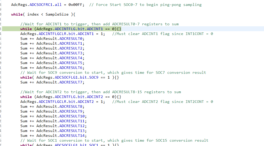
然会会卡死在(见图)
