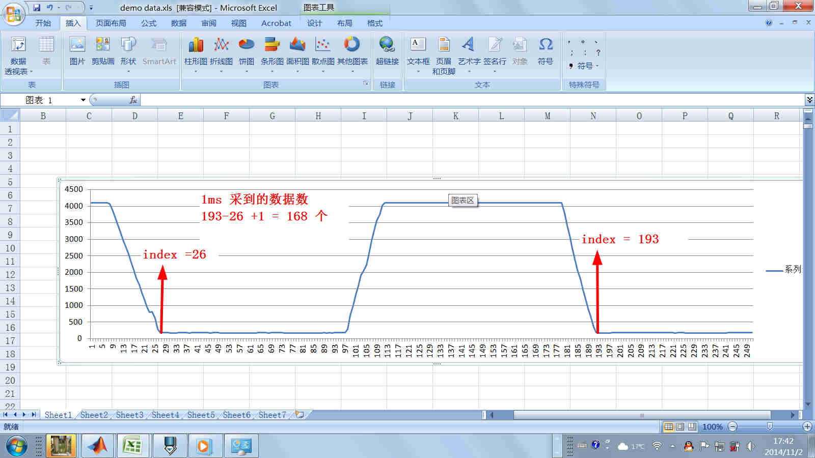
F28335技术手册上面说,内部ADC最高采样率顺序采样可达到8M左右,同步采样可以达到4M左右,我采用的PWM触发其ADC同步采样,只读取一个通道的值,最高采样率可以达到750K,却提高不上去了,ADC时钟设置最高和采样保持时间设置最短,请问F28335技术手册上面说的那么高的采样率怎么达到哈?或者F28335技术手册上面的几M采样率是几个通道合起来的采样率?请各位大神帮忙解决,谢谢!
This thread has been locked.
If you have a related question, please click the "Ask a related question" button in the top right corner. The newly created question will be automatically linked to this question.
我这里是采4个通道,每个通道 600多K,和你的采用PWM方式不一样,我采用的方法是用一个脉冲产生AD转换,然后AD自动转换,DMA送到内存。
/***************************************************************************
If the cascaded SEQ was executed, the results would go to the following ADCRESULT registers:
ADCINA0 -> ADCRESULT0
ADCINB0 -> ADCRESULT1
ADCINA1 -> ADCRESULT2
ADCINB1 -> ADCRESULT3
ADCINA2 -> ADCRESULT4
ADCINB2 -> ADCRESULT5
ADCINA3 -> ADCRESULT6
ADCINB3 -> ADCRESULT7
ADCINA4 -> ADCRESULT8
ADCINB4 -> ADCRESULT9
ADCINA5 -> ADCRESULT10
ADCINB5 -> ADCRESULT11
ADCINA6 -> ADCRESULT12
ADCINB6 -> ADCRESULT13
ADCINA7 -> ADCRESULT14
ADCINB7 -> ADCRESULT15
****************************************************************************/
void ADCConfig(void)
{
//InitAdc();
//AdcRegs.ADCREFSEL.bit.REF_SEL = 0x0; // 00,Internal reference selected (default)
//AdcRegs.ADCTRL1.bit.ACQ_PS = 0xF; // This bit field controls the width of SOC pulse,
//AdcRegs.ADCTRL1.bit.CONT_RUN = 0; // 0/1:Start-stop mode/Continuous conversion mode
//AdcRegs.ADCTRL1.bit.SEQ_OVRD = 0; // Sequencer override Disabled,Allows the sequencer to wrap around at the end of conversions set by MAX_CONVn
//AdcRegs.ADCTRL1.bit.SEQ_CASC = 1; // Cascaded mode. SEQ1 and SEQ2 operate as a single 16-state sequencer (SEQ).
//AdcRegs.ADCTRL1.bit.CPS = 0; // 0:ADCCLK = Fclk/1; 1:ADCCLK = Fclk/2; Fclk = Prescaled HISPCLK; NOTE: HISPCLK = SYSCLKOUT/2,
//AdcRegs.ADCTRL2.bit.EPWM_SOCA_SEQ1 = 1; // Setting this bit allows the cascaded sequencer to be started by an ePWM SOCB signal
//AdcRegs.ADCTRL2.bit.RST_SEQ1 = 1; // Immediately reset sequencer to state CONV00
//AdcRegs.ADCTRL2.bit.INT_ENA_SEQ1 = 1; // Interrupt request by INT_SEQ1 is enabled.
//AdcRegs.ADCTRL3.bit.ADCCLKPS = 0x3; // Core clock divider, HISPCLK = SYSCLKOUT/2, 75M/6 = 12.5Mhz, 12.5M/(0+1) = 12.5Mhz,
//AdcRegs.ADCTRL3.bit.SMODE_SEL = 1; // 0/1,Sequential/Simultaneous sampling mode is selected
//AdcRegs.ADCMAXCONV.all = 0; //AdcRegs.ADCCHSELSEQ1.bit.CONV00 = 0; // ADC Input Channel Selected
InitAdc();
AdcRegs.ADCTRL3.bit.SMODE_SEL = 1; // 0/1,Sequential/Simultaneous sampling mode is selected
AdcRegs.ADCTRL1.bit.SEQ_CASC = 1; // 0/1,separate mode/ Cascaded mode. SEQ1 and SEQ2 operate as a single 16-state sequencer (SEQ).
AdcRegs.ADCMAXCONV.all = 0x07; // 8 double conv's (4 total),The sequence naturally wraps around at the end of the MAX_CONVn setting.
AdcRegs.ADCREFSEL.bit.REF_SEL = 0x0; // 00,Internal reference selected (default)
AdcRegs.ADCTRL1.bit.ACQ_PS = 0x1; // This bit field controls the width of SOC pulse,0x0F
AdcRegs.ADCTRL1.bit.CONT_RUN = 1; // 0/1:Start-stop mode/Continuous conversion mode
AdcRegs.ADCTRL1.bit.SEQ_OVRD = 0; // Sequencer override Disabled,Allows the sequencer to wrap around at the end of conversions set by MAX_CONVn
AdcRegs.ADCTRL1.bit.CPS = 0; // 0:ADCCLK = Fclk/1; 1:ADCCLK = Fclk/2; Fclk = Prescaled HISPCLK; NOTE: HISPCLK = SYSCLKOUT/2,
//AdcRegs.ADCTRL2.bit.EPWM_SOCA_SEQ1 = 0; // Setting this bit allows the cascaded sequencer to be started by an ePWM SOCA signal
AdcRegs.ADCTRL2.bit.RST_SEQ1 = 1; // Immediately reset sequencer to state CONV00
AdcRegs.ADCTRL2.bit.INT_ENA_SEQ1 = 1; // Interrupt request by INT_SEQ1 is enabled to trigger DMA transfer, no need to implement SEQ1 ISA
AdcRegs.ADCTRL3.bit.ADCCLKPS = 0x2; // Core clock divider, HISPCLK = SYSCLKOUT/2, 75M/6 = 12.5Mhz, 12.5M/(0+1) = 12.5Mhz
// ACQ_PS = 0x01, ADCCLKPS = 0x0 can not convert analog correctly
// ACQ_PS = 0x01, ADCCLKPS = 0x1 615k samples /second
// ACQ_PS = 0x01, ADCCLKPS = 0x2 590K samples /second
// ACQ_PS = 0x01, ADCCLKPS = 0x3 390K samples /second
// ACQ_PS = 0x01, ADCCLKPS = 0x4 290K samples /second
// ACQ_PS = 0x01, ADCCLKPS = 0x5 232K samples /second
// ACQ_PS = 0x01, ADCCLKPS = 0x6 194K samples /second
// ACQ_PS = 0x01, ADCCLKPS = 0x7 164K samples /second
// ACQ_PS = 0x01, ADCCLKPS = 0x8 143K samples /second
// ACQ_PS = 0x01, ADCCLKPS = 0x9 130K samples /second
// ACQ_PS = 0x01, ADCCLKPS = 0xA 114K samples /second
// ACQ_PS = 0x01, ADCCLKPS = 0xB 104K samples /second
// ACQ_PS = 0xF, ADCCLKPS = 0x3 15K samples /second
AdcRegs.ADCCHSELSEQ1.bit.CONV00 = 0x0; // ADC Input Channel Selected,ADCINA0/ADCINB0
AdcRegs.ADCCHSELSEQ1.bit.CONV01 = 0x1; // ADC Input Channel Selected,ADCINA1/ADCINB1
AdcRegs.ADCCHSELSEQ1.bit.CONV02 = 0x0; // ADC Input Channel Selected,ADCINA0/ADCINB0
AdcRegs.ADCCHSELSEQ1.bit.CONV03 = 0x1; // ADC Input Channel Selected,ADCINA1/ADCINB1
AdcRegs.ADCCHSELSEQ2.bit.CONV04 = 0x0; // ADC Input Channel Selected,ADCINA0/ADCINB0
AdcRegs.ADCCHSELSEQ2.bit.CONV05 = 0x1; // ADC Input Channel Selected,ADCINA1/ADCINB1
AdcRegs.ADCCHSELSEQ2.bit.CONV06 = 0x0; // ADC Input Channel Selected,ADCINA0/ADCINB0
AdcRegs.ADCCHSELSEQ2.bit.CONV07 = 0x1; // ADC Input Channel Selected,ADCINA1/ADCINB1
}
希望对你有帮助