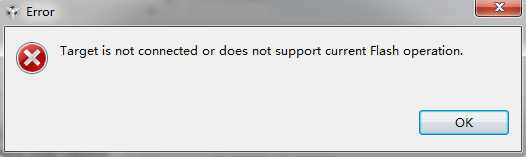
在调试F28M35时候,M3的程序能够正常下载到flash上,而C28不能下载,ccs 6提示的错误信息为:
C28xx_0: Loader: One or more sections of your program falls into a memory region that is not writable. These regions will not actually be written to the target. Check your linker configuration and/or memory map.
C28xx_0: File Loader: Verification failed: Values at address 0x000000000013E000 do not match Please verify target memory and memory map.
C28xx_0: GEL: File: C:\Users\MQinDong\Documents\TIccs\Projects\MMC\MMC_v2\MMC_C28_v2\FLASH\MMC_C28_v2.out: a data verification error occurred, file load failed.
我用的cmd文件是controlSUITE提供的最新版本(v206):F28M35x_headers/cmd/F28M35x_Headers_nonBIOS.cmd和F28M35x_common\cmd\F28M35H52C1_c28.cmd.
其中,F28M35H52C1_c28.cmd如下。
MEMORY
{
PAGE 0: /* Program Memory */
/* Memory (RAM/FLASH/OTP) blocks can be moved to PAGE1 for data allocation */
RAML0 : origin = 0x008000, length = 0x001000 /* on-chip RAM block L0 */
RAML1 : origin = 0x009000, length = 0x001000 /* on-chip RAM block L1 */
FLASHN : origin = 0x100000, length = 0x002000 /* on-chip FLASH */
FLASHM : origin = 0x102000, length = 0x002000 /* on-chip FLASH */
FLASHL : origin = 0x104000, length = 0x002000 /* on-chip FLASH */
FLASHK : origin = 0x106000, length = 0x002000 /* on-chip FLASH */
FLASHJ : origin = 0x108000, length = 0x008000 /* on-chip FLASH */
FLASHI : origin = 0x110000, length = 0x008000 /* on-chip FLASH */
FLASHH : origin = 0x118000, length = 0x008000 /* on-chip FLASH */
FLASHG : origin = 0x120000, length = 0x008000 /* on-chip FLASH */
FLASHF : origin = 0x128000, length = 0x008000 /* on-chip FLASH */
FLASHE : origin = 0x130000, length = 0x008000 /* on-chip FLASH */
FLASHD : origin = 0x138000, length = 0x002000 /* on-chip FLASH */
FLASHC : origin = 0x13A000, length = 0x002000 /* on-chip FLASH */
FLASHA : origin = 0x13E000, length = 0x001F80 /* on-chip FLASH */
CSM_RSVD : origin = 0x13FF80, length = 0x000070 /* Part of FLASHA. Program with all 0x0000 when CSM is in use. */
BEGIN : origin = 0x13FFF0, length = 0x000002 /* Part of FLASHA. Used for "boot to Flash" bootloader mode. */
FLASH_EXE_ONLY_P0 : origin = 0x13FFF2, length = 0x000002 /* Part of FLASHA. Flash execute only locations in FLASHA */
ECSL_PWL_P0 : origin = 0x13FFF4, length = 0x000004 /* Part of FLASHA. ECSL password locations in FLASHA */
CSM_PWL_P0 : origin = 0x13FFF8, length = 0x000008 /* Part of FLASHA. CSM password locations in FLASHA */
FPUTABLES : origin = 0x3FD258, length = 0x0006A0 /* FPU Tables in Boot ROM */
IQTABLES : origin = 0x3FD8F8, length = 0x000B50 /* IQ Math Tables in Boot ROM */
IQTABLES2 : origin = 0x3FE448, length = 0x00008C /* IQ Math Tables in Boot ROM */
IQTABLES3 : origin = 0x3FE4D4, length = 0x0000AA /* IQ Math Tables in Boot ROM */
BOOTROM : origin = 0x3FEDA8, length = 0x001200 /* Boot ROM */
PIEMISHNDLR : origin = 0x3FFFBE, length = 0x000002 /* part of boot ROM */
RESET : origin = 0x3FFFC0, length = 0x000002 /* part of boot ROM */
VECTORS : origin = 0x3FFFC2, length = 0x00003E /* part of boot ROM */
PAGE 1 : /* Data Memory */
/* Memory (RAM/FLASH/OTP) blocks can be moved to PAGE0 for program allocation */
/* Registers remain on PAGE1 */
BOOT_RSVD : origin = 0x000000, length = 0x000050 /* Part of M0, BOOT rom will use this for stack */
RAMM0 : origin = 0x000050, length = 0x0003B0 /* on-chip RAM block M0 */
RAMM1 : origin = 0x000400, length = 0x000400 /* on-chip RAM block M1 */
RAML2 : origin = 0x00A000, length = 0x001000 /* on-chip RAM block L2 */
RAML3 : origin = 0x00B000, length = 0x001000 /* on-chip RAM block L3 */
RAMS0 : origin = 0x00C000, length = 0x001000 /* on-chip Shared RAM block S0 */
RAMS1 : origin = 0x00D000, length = 0x001000 /* on-chip Shared RAM block S1 */
RAMS2 : origin = 0x00E000, length = 0x001000 /* on-chip Shared RAM block S2 */
RAMS3 : origin = 0x00F000, length = 0x001000 /* on-chip Shared RAM block S3 */
RAMS4 : origin = 0x010000, length = 0x001000 /* on-chip Shared RAM block S4 */
RAMS5 : origin = 0x011000, length = 0x001000 /* on-chip Shared RAM block S5 */
RAMS6 : origin = 0x012000, length = 0x001000 /* on-chip Shared RAM block S6 */
RAMS7 : origin = 0x013000, length = 0x001000 /* on-chip Shared RAM block S7 */
CTOMRAM : origin = 0x03F800, length = 0x000380 /* C28 to M3 Message RAM */
MTOCRAM : origin = 0x03FC00, length = 0x000380 /* M3 to C28 Message RAM */
FLASHB : origin = 0x13C000, length = 0x002000 /* on-chip FLASH */
}
/* Allocate sections to memory blocks.
Note:
codestart user defined section in DSP28_CodeStartBranch.asm used to redirect code
execution when booting to flash
ramfuncs user defined section to store functions that will be copied from Flash into RAM
*/
SECTIONS
{
/* Allocate program areas: */
.cinit : > FLASHA PAGE = 0
.pinit : > FLASHA, PAGE = 0
.text : > FLASHA PAGE = 0
codestart : > BEGIN PAGE = 0
ramfuncs : LOAD = FLASHD,
RUN = RAML0,
LOAD_START(_RamfuncsLoadStart),
LOAD_SIZE(_RamfuncsLoadSize),
LOAD_END(_RamfuncsLoadEnd),
RUN_START(_RamfuncsRunStart),
RUN_SIZE(_RamfuncsRunSize),
RUN_END(_RamfuncsRunEnd),
PAGE = 0
flashexeonly : > FLASH_EXE_ONLY_P0 PAGE = 0
ecslpasswds : > ECSL_PWL_P0 PAGE = 0
csmpasswds : > CSM_PWL_P0 PAGE = 0
csm_rsvd : > CSM_RSVD PAGE = 0
/* The following section definitions are required when using the IPC API Drivers */
GROUP : > CTOMRAM, PAGE = 1
{
PUTBUFFER
PUTWRITEIDX
GETREADIDX
}
GROUP : > MTOCRAM, PAGE = 1
{
GETBUFFER : TYPE = DSECT
GETWRITEIDX : TYPE = DSECT
PUTREADIDX : TYPE = DSECT
}
/* Allocate uninitalized data sections: */
.stack : > RAMM0 PAGE = 1
.ebss : > RAML2 PAGE = 1
.esysmem : > RAML2 PAGE = 1
/* Initalized sections go in Flash */
/* For SDFlash to program these, they must be allocated to page 0 */
.econst : > FLASHA PAGE = 0
.switch : > FLASHA PAGE = 0
/* Allocate IQ math areas: */
IQmath : > FLASHA PAGE = 0 /* Math Code */
IQmathTables : > IQTABLES, PAGE = 0, TYPE = NOLOAD
/* Allocate FPU math areas: */
FPUmathTables : > FPUTABLES, PAGE = 0, TYPE = NOLOAD
DMARAML2 : > RAML2, PAGE = 1
DMARAML3 : > RAML3, PAGE = 1
/* Uncomment the section below if calling the IQNexp() or IQexp()
functions from the IQMath.lib library in order to utilize the
relevant IQ Math table in Boot ROM (This saves space and Boot ROM
is 1 wait-state). If this section is not uncommented, IQmathTables2
will be loaded into other memory (SARAM, Flash, etc.) and will take
up space, but 0 wait-state is possible.
*/
/*
IQmathTables2 : > IQTABLES2, PAGE = 0, TYPE = NOLOAD
{
IQmath.lib<IQNexpTable.obj> (IQmathTablesRam)
}
*/
/* Uncomment the section below if calling the IQNasin() or IQasin()
functions from the IQMath.lib library in order to utilize the
relevant IQ Math table in Boot ROM (This saves space and Boot ROM
is 1 wait-state). If this section is not uncommented, IQmathTables2
will be loaded into other memory (SARAM, Flash, etc.) and will take
up space, but 0 wait-state is possible.
*/
/*
IQmathTables3 : > IQTABLES3, PAGE = 0, TYPE = NOLOAD
{
IQmath.lib<IQNasinTable.obj> (IQmathTablesRam)
}
*/
/* .reset is a standard section used by the compiler. It contains the */
/* the address of the start of _c_int00 for C Code. /*
/* When using the boot ROM this section and the CPU vector */
/* table is not needed. Thus the default type is set here to */
/* DSECT */
.reset : > RESET, PAGE = 0, TYPE = DSECT
vectors : > VECTORS PAGE = 0, TYPE = DSECT
}