
This thread has been locked.
If you have a related question, please click the "Ask a related question" button in the top right corner. The newly created question will be automatically linked to this question.
测量所有 MibSPI 从 DMA 传输开始到结束的周期时间显示为1、8ms。 测量从 DMA 传输开始到结束的后续周期的周期时间显示为3、0ms。 请参阅以下代码。 在初始化阶段之后、代码进入一个 while (1)循环。 在此循环中、将 HBC 标志考虑在内、所有4个 MibSP 都将连续启动。 开始时、PWM 信号设置为100%占空比、并且在所有 DMA 通道完成传输后、PWM 信号设置为1%占空比。 100%占空比通过数字存储示波器进行测量。 对于第一个 while 环路周期、可以测量1、8ms。 但对于所有后续 while 环路周期、测量值为3、0ms。 有没有人知道为什么会有这样的差异?
/* USER CODE BEGIN (0) */
/* USER CODE END */

/* Include Files */

#include "HL_sys_common.h"

/* USER CODE BEGIN (1) */
#include "HL_mibspi.h"
#include "HL_sys_dma.h"
#include "HL_het.h"
#include "HL_reg_het.h"

/* example data Pattern configuration */
#define D_SIZE      128
#define BUFFER_SIZE 1024

void loadDataPattern(uint32 psize, uint16* pptr);
void mibspiEnableInternalLoopback(mibspiBASE_t *mibspi);
void dmaConfigCtrlPacket(uint32 sadd,uint32 dadd,uint32 dsize);
void mibspiDmaConfig(mibspiBASE_t *mibspi,uint32 channel, uint32 txchannel, uint32 rxchannel);

#pragma SET_DATA_SECTION(".sharedRAM")
uint16 TXDATA[BUFFER_SIZE];         /* transmit buffer in sys ram */
uint16 RXDATA[BUFFER_SIZE]= {0};    /* receive  buffer in sys ram */
uint16 TXDATA2[BUFFER_SIZE];         /* transmit buffer in sys ram */
uint16 RXDATA2[BUFFER_SIZE]= {0};    /* receive  buffer in sys ram */
uint16 TXDATA3[BUFFER_SIZE];         /* transmit buffer in sys ram */
uint16 RXDATA3[BUFFER_SIZE]= {0};    /* receive  buffer in sys ram */
uint16 TXDATA4[BUFFER_SIZE];         /* transmit buffer in sys ram */
uint16 RXDATA4[BUFFER_SIZE]= {0};    /* receive  buffer in sys ram */
#pragma SET_DATA_SECTION()

static g_dmaCTRL g_dmaCTRLPKT1, g_dmaCTRLPKT2;    /* dma control packet configuration stack */


/* USER CODE END */

/** @fn void main(void)
*   @brief Application main function
*   @note This function is empty by default.
*
*   This function is called after startup.
*   The user can use this function to implement the application.
*/

/* USER CODE BEGIN (2) */
/* USER CODE END */

void main(void)
{
/* USER CODE BEGIN (3) */

   uint32 i;
   uint32 j;
   uint32 m;

   /* - creating a data chunk in system ram to start with ... */
   loadDataPattern(BUFFER_SIZE,&TXDATA[0]);
   loadDataPattern(BUFFER_SIZE,&TXDATA2[0]);
   loadDataPattern(BUFFER_SIZE,&TXDATA3[0]);
   loadDataPattern(BUFFER_SIZE,&TXDATA4[0]);

   clearDataPattern(BUFFER_SIZE,&RXDATA[0]);
   clearDataPattern(BUFFER_SIZE,&RXDATA2[0]);
   clearDataPattern(BUFFER_SIZE,&RXDATA3[0]);
   clearDataPattern(BUFFER_SIZE,&RXDATA4[0]);

   /* - initializing mibspi - enabling tg 0 , length 127 (halcogen file)*/
   mibspiInit();

   /* - enabling loopback ( this is to emulate data transfer without external wires */
   mibspiEnableInternalLoopback(mibspiREG1);
   mibspiEnableInternalLoopback(mibspiREG2);
   mibspiEnableInternalLoopback(mibspiREG3);
   mibspiEnableInternalLoopback(mibspiREG4);

   /* - configuring dma control packets   */
   g_dmaCTRLPKT1.SADD      = (uint32)TXDATA;    /* source address             */
   g_dmaCTRLPKT1.DADD      = (uint32)&(mibspiRAM1->tx[0].data);    /* destination  address       */
   g_dmaCTRLPKT1.CHCTRL    = 0;                 /* channel control            */
   g_dmaCTRLPKT1.FRCNT	   = 8;//1;                 /* frame count                */
   g_dmaCTRLPKT1.ELCNT     = 32;//D_SIZE;            /* element count              */
   g_dmaCTRLPKT1.ELDOFFSET = 4;                 /* element destination offset */
   g_dmaCTRLPKT1.ELSOFFSET = 0;		            /* element destination offset */
   g_dmaCTRLPKT1.FRDOFFSET = 0;		            /* frame destination offset   */
   g_dmaCTRLPKT1.FRSOFFSET = 0;                 /* frame destination offset   */
   g_dmaCTRLPKT1.PORTASGN  = PORTA_READ_PORTB_WRITE;
   g_dmaCTRLPKT1.RDSIZE    = ACCESS_64_BIT;	    /* read size                  */
   g_dmaCTRLPKT1.WRSIZE    = ACCESS_16_BIT; 	/* write size                 */
   g_dmaCTRLPKT1.TTYPE     = FRAME_TRANSFER ;   /* transfer type              */
   g_dmaCTRLPKT1.ADDMODERD = ADDR_INC1;         /* address mode read          */
   g_dmaCTRLPKT1.ADDMODEWR = ADDR_OFFSET;       /* address mode write         */
   g_dmaCTRLPKT1.AUTOINIT  = AUTOINIT_ON;       /* autoinit                   */

   g_dmaCTRLPKT2.SADD      = (uint32)&(mibspiRAM1->rx[0].data);    /* source address             */
   g_dmaCTRLPKT2.DADD      = (uint32)RXDATA;    /* destination  address       */
   g_dmaCTRLPKT2.CHCTRL    = 0;                 /* channel control            */
   g_dmaCTRLPKT2.FRCNT	   = 8;//1;                 /* frame count                */
   g_dmaCTRLPKT2.ELCNT     = D_SIZE;             /* element count              */
   g_dmaCTRLPKT2.ELDOFFSET = 0;                 /* element destination offset */
   g_dmaCTRLPKT2.ELSOFFSET = 4;		            /* element destination offset */
   g_dmaCTRLPKT2.FRDOFFSET = 0;		            /* frame destination offset   */
   g_dmaCTRLPKT2.FRSOFFSET = 0;                 /* frame destination offset   */
   g_dmaCTRLPKT2.PORTASGN  = PORTB_READ_PORTA_WRITE;
   g_dmaCTRLPKT2.RDSIZE    = ACCESS_16_BIT;	    /* read size                  */
   g_dmaCTRLPKT2.WRSIZE    = ACCESS_64_BIT; 	/* write size                 */
   g_dmaCTRLPKT2.TTYPE     = FRAME_TRANSFER ;   /* transfer type              */
   g_dmaCTRLPKT2.ADDMODERD = ADDR_OFFSET;         /* address mode read          */
   g_dmaCTRLPKT2.ADDMODEWR = ADDR_INC1;       /* address mode write         */
   g_dmaCTRLPKT2.AUTOINIT  = AUTOINIT_ON;       /* autoinit                   */

   /* upto 32 control packets are supported. */

   /* - setting dma control packets */
   dmaSetCtrlPacket(DMA_CH0,g_dmaCTRLPKT2);
   dmaSetCtrlPacket(DMA_CH1,g_dmaCTRLPKT1);

   /* - setting the dma channel to trigger on h/w request */
   dmaSetChEnable(DMA_CH0, DMA_HW);
   dmaSetChEnable(DMA_CH1, DMA_HW);

   /* - configuring dma control packets   */
   g_dmaCTRLPKT1.SADD      = (uint32)TXDATA2;    /* source address             */
   g_dmaCTRLPKT1.DADD      = (uint32)&(mibspiRAM2->tx[0].data);    /* destination  address       */
   g_dmaCTRLPKT1.CHCTRL    = 0;                 /* channel control            */
   g_dmaCTRLPKT1.FRCNT     = 8;//1;                 /* frame count                */
   g_dmaCTRLPKT1.ELCNT     = 32;//D_SIZE;            /* element count              */
   g_dmaCTRLPKT1.ELDOFFSET = 4;                 /* element destination offset */
   g_dmaCTRLPKT1.ELSOFFSET = 0;                 /* element destination offset */
   g_dmaCTRLPKT1.FRDOFFSET = 0;                 /* frame destination offset   */
   g_dmaCTRLPKT1.FRSOFFSET = 0;                 /* frame destination offset   */
   g_dmaCTRLPKT1.PORTASGN  = PORTA_READ_PORTB_WRITE;
   g_dmaCTRLPKT1.RDSIZE    = ACCESS_64_BIT;     /* read size                  */
   g_dmaCTRLPKT1.WRSIZE    = ACCESS_16_BIT;     /* write size                 */
   g_dmaCTRLPKT1.TTYPE     = FRAME_TRANSFER ;   /* transfer type              */
   g_dmaCTRLPKT1.ADDMODERD = ADDR_INC1;         /* address mode read          */
   g_dmaCTRLPKT1.ADDMODEWR = ADDR_OFFSET;       /* address mode write         */
   g_dmaCTRLPKT1.AUTOINIT  = AUTOINIT_ON;       /* autoinit                   */

   g_dmaCTRLPKT2.SADD      = (uint32)&(mibspiRAM2->rx[0].data);    /* source address             */
   g_dmaCTRLPKT2.DADD      = (uint32)RXDATA2;    /* destination  address       */
   g_dmaCTRLPKT2.CHCTRL    = 0;                 /* channel control            */
   g_dmaCTRLPKT2.FRCNT     = 8;//1;                 /* frame count                */
   g_dmaCTRLPKT2.ELCNT     = D_SIZE;             /* element count              */
   g_dmaCTRLPKT2.ELDOFFSET = 0;                 /* element destination offset */
   g_dmaCTRLPKT2.ELSOFFSET = 4;                 /* element destination offset */
   g_dmaCTRLPKT2.FRDOFFSET = 0;                 /* frame destination offset   */
   g_dmaCTRLPKT2.FRSOFFSET = 0;                 /* frame destination offset   */
   g_dmaCTRLPKT2.PORTASGN  = PORTB_READ_PORTA_WRITE;
   g_dmaCTRLPKT2.RDSIZE    = ACCESS_16_BIT;     /* read size                  */
   g_dmaCTRLPKT2.WRSIZE    = ACCESS_64_BIT;     /* write size                 */
   g_dmaCTRLPKT2.TTYPE     = FRAME_TRANSFER ;   /* transfer type              */
   g_dmaCTRLPKT2.ADDMODERD = ADDR_OFFSET;         /* address mode read          */
   g_dmaCTRLPKT2.ADDMODEWR = ADDR_INC1;       /* address mode write         */
   g_dmaCTRLPKT2.AUTOINIT  = AUTOINIT_ON;       /* autoinit                   */

   /* upto 32 control packets are supported. */

   /* - setting dma control packets */
   dmaSetCtrlPacket(DMA_CH2,g_dmaCTRLPKT2);
   dmaSetCtrlPacket(DMA_CH3,g_dmaCTRLPKT1);

   /* - setting the dma channel to trigger on h/w request */
   dmaSetChEnable(DMA_CH2, DMA_HW);
   dmaSetChEnable(DMA_CH3, DMA_HW);

   /* - configuring dma control packets   */
   g_dmaCTRLPKT1.SADD      = (uint32)TXDATA3;    /* source address             */
   g_dmaCTRLPKT1.DADD      = (uint32)&(mibspiRAM3->tx[0].data);    /* destination  address       */
   g_dmaCTRLPKT1.CHCTRL    = 0;                 /* channel control            */
   g_dmaCTRLPKT1.FRCNT     = 8;//1;                 /* frame count                */
   g_dmaCTRLPKT1.ELCNT     = 32;//D_SIZE;            /* element count              */
   g_dmaCTRLPKT1.ELDOFFSET = 4;                 /* element destination offset */
   g_dmaCTRLPKT1.ELSOFFSET = 0;                 /* element destination offset */
   g_dmaCTRLPKT1.FRDOFFSET = 0;                 /* frame destination offset   */
   g_dmaCTRLPKT1.FRSOFFSET = 0;                 /* frame destination offset   */
   g_dmaCTRLPKT1.PORTASGN  = PORTA_READ_PORTB_WRITE;
   g_dmaCTRLPKT1.RDSIZE    = ACCESS_64_BIT;     /* read size                  */
   g_dmaCTRLPKT1.WRSIZE    = ACCESS_16_BIT;     /* write size                 */
   g_dmaCTRLPKT1.TTYPE     = FRAME_TRANSFER ;   /* transfer type              */
   g_dmaCTRLPKT1.ADDMODERD = ADDR_INC1;         /* address mode read          */
   g_dmaCTRLPKT1.ADDMODEWR = ADDR_OFFSET;       /* address mode write         */
   g_dmaCTRLPKT1.AUTOINIT  = AUTOINIT_ON;       /* autoinit                   */

   g_dmaCTRLPKT2.SADD      = (uint32)&(mibspiRAM3->rx[0].data);    /* source address             */
   g_dmaCTRLPKT2.DADD      = (uint32)RXDATA3;    /* destination  address       */
   g_dmaCTRLPKT2.CHCTRL    = 0;                 /* channel control            */
   g_dmaCTRLPKT2.FRCNT     = 8;//1;                 /* frame count                */
   g_dmaCTRLPKT2.ELCNT     = D_SIZE;             /* element count              */
   g_dmaCTRLPKT2.ELDOFFSET = 0;                 /* element destination offset */
   g_dmaCTRLPKT2.ELSOFFSET = 4;                 /* element destination offset */
   g_dmaCTRLPKT2.FRDOFFSET = 0;                 /* frame destination offset   */
   g_dmaCTRLPKT2.FRSOFFSET = 0;                 /* frame destination offset   */
   g_dmaCTRLPKT2.PORTASGN  = PORTB_READ_PORTA_WRITE;
   g_dmaCTRLPKT2.RDSIZE    = ACCESS_16_BIT;     /* read size                  */
   g_dmaCTRLPKT2.WRSIZE    = ACCESS_64_BIT;     /* write size                 */
   g_dmaCTRLPKT2.TTYPE     = FRAME_TRANSFER ;   /* transfer type              */
   g_dmaCTRLPKT2.ADDMODERD = ADDR_OFFSET;         /* address mode read          */
   g_dmaCTRLPKT2.ADDMODEWR = ADDR_INC1;       /* address mode write         */
   g_dmaCTRLPKT2.AUTOINIT  = AUTOINIT_ON;       /* autoinit                   */

   /* upto 32 control packets are supported. */

   /* - setting dma control packets */
   dmaSetCtrlPacket(DMA_CH4,g_dmaCTRLPKT2);
   dmaSetCtrlPacket(DMA_CH5,g_dmaCTRLPKT1);

   dmaReqAssign(DMA_CH4, DMA_REQ14);
   dmaReqAssign(DMA_CH5, DMA_REQ15);

   /* - setting the dma channel to trigger on h/w request */
   dmaSetChEnable(DMA_CH4, DMA_HW);
   dmaSetChEnable(DMA_CH5, DMA_HW);

   /* - configuring dma control packets   */
   g_dmaCTRLPKT1.SADD      = (uint32)TXDATA4;    /* source address             */
   g_dmaCTRLPKT1.DADD      = (uint32)&(mibspiRAM4->tx[0].data);    /* destination  address       */
   g_dmaCTRLPKT1.CHCTRL    = 0;                 /* channel control            */
   g_dmaCTRLPKT1.FRCNT     = 8;//1;                 /* frame count                */
   g_dmaCTRLPKT1.ELCNT     = 32;//D_SIZE;            /* element count              */
   g_dmaCTRLPKT1.ELDOFFSET = 4;                 /* element destination offset */
   g_dmaCTRLPKT1.ELSOFFSET = 0;                 /* element destination offset */
   g_dmaCTRLPKT1.FRDOFFSET = 0;                 /* frame destination offset   */
   g_dmaCTRLPKT1.FRSOFFSET = 0;                 /* frame destination offset   */
   g_dmaCTRLPKT1.PORTASGN  = PORTA_READ_PORTB_WRITE;
   g_dmaCTRLPKT1.RDSIZE    = ACCESS_64_BIT;     /* read size                  */
   g_dmaCTRLPKT1.WRSIZE    = ACCESS_16_BIT;     /* write size                 */
   g_dmaCTRLPKT1.TTYPE     = FRAME_TRANSFER ;   /* transfer type              */
   g_dmaCTRLPKT1.ADDMODERD = ADDR_INC1;         /* address mode read          */
   g_dmaCTRLPKT1.ADDMODEWR = ADDR_OFFSET;       /* address mode write         */
   g_dmaCTRLPKT1.AUTOINIT  = AUTOINIT_ON;       /* autoinit                   */

   g_dmaCTRLPKT2.SADD      = (uint32)&(mibspiRAM4->rx[0].data);    /* source address             */
   g_dmaCTRLPKT2.DADD      = (uint32)RXDATA4;    /* destination  address       */
   g_dmaCTRLPKT2.CHCTRL    = 0;                 /* channel control            */
   g_dmaCTRLPKT2.FRCNT     = 8;//1;                 /* frame count                */
   g_dmaCTRLPKT2.ELCNT     = D_SIZE;             /* element count              */
   g_dmaCTRLPKT2.ELDOFFSET = 0;                 /* element destination offset */
   g_dmaCTRLPKT2.ELSOFFSET = 4;                 /* element destination offset */
   g_dmaCTRLPKT2.FRDOFFSET = 0;                 /* frame destination offset   */
   g_dmaCTRLPKT2.FRSOFFSET = 0;                 /* frame destination offset   */
   g_dmaCTRLPKT2.PORTASGN  = PORTB_READ_PORTA_WRITE;
   g_dmaCTRLPKT2.RDSIZE    = ACCESS_16_BIT;     /* read size                  */
   g_dmaCTRLPKT2.WRSIZE    = ACCESS_64_BIT;     /* write size                 */
   g_dmaCTRLPKT2.TTYPE     = FRAME_TRANSFER ;   /* transfer type              */
   g_dmaCTRLPKT2.ADDMODERD = ADDR_OFFSET;         /* address mode read          */
   g_dmaCTRLPKT2.ADDMODEWR = ADDR_INC1;       /* address mode write         */
   g_dmaCTRLPKT2.AUTOINIT  = AUTOINIT_ON;       /* autoinit                   */

   /* upto 32 control packets are supported. */

   /* - setting dma control packets */
   dmaSetCtrlPacket(DMA_CH6,g_dmaCTRLPKT2);
   dmaSetCtrlPacket(DMA_CH7,g_dmaCTRLPKT1);

   dmaReqAssign(DMA_CH6, DMA_REQ24);
   dmaReqAssign(DMA_CH7, DMA_REQ25);

   /* - setting the dma channel to trigger on h/w request */
   dmaSetChEnable(DMA_CH6, DMA_HW);
   dmaSetChEnable(DMA_CH7, DMA_HW);

   //dmaReqAssign(DMA_CH0, DMA_REQ0);
   //dmaReqAssign(DMA_CH1, DMA_REQ1);

   /* - configuring the mibspi dma , channel 0 , tx line -0 , rxline -1     */
   /* - refer to the device data sheet dma request source for mibspi tx/rx  */
   mibspiDmaConfig(mibspiREG1,0,0,1);
   mibspiDmaConfig(mibspiREG2,0,0,1);
   mibspiDmaConfig(mibspiREG3,0,0,1);
   mibspiDmaConfig(mibspiREG4,0,0,1);

   dmaEnable();
   hetInit();
   pwmSetDuty(hetRAM1, 0, 1);

   i = 0;

while(1)
{
   i++;

   pwmSetDuty(hetRAM1, 0, 100);

   /* - start the mibspi transfer tg 0 */
   mibspiTransfer(mibspiREG1,0 );

   while(dmaGetInterruptStatus(DMA_CH0, HBC) == FALSE);

   mibspiTransfer(mibspiREG2,0 );

   //while(dmaGetInterruptStatus(DMA_CH0, BTC) == FALSE);
   while(dmaGetInterruptStatus(DMA_CH2, HBC) == FALSE);

   mibspiTransfer(mibspiREG3,0 );

   while(dmaGetInterruptStatus(DMA_CH4, HBC) == FALSE);

   mibspiTransfer(mibspiREG4,0 );

   while(dmaGetInterruptStatus(DMA_CH6, BTC) == FALSE);

   //while(dmaGetInterruptStatus(DMA_CH6, BTC) == FALSE);
   //while(dmaGetInterruptStatus(DMA_CH0, BTC) == FALSE);
   //while(dmaGetInterruptStatus(DMA_CH2, BTC) == FALSE);
   //while(dmaGetInterruptStatus(DMA_CH4, BTC) == FALSE);

   pwmSetDuty(hetRAM1, 0, 1);

   mibspiDisableTransfer(mibspiREG1,0);
   mibspiDisableTransfer(mibspiREG2,0);
   mibspiDisableTransfer(mibspiREG3,0);
   mibspiDisableTransfer(mibspiREG4,0);

   dmaREG->BTCFLAG = 0xFFFFFFFF;
   dmaREG->HBCFLAG = 0xFFFFFFFF;

   dmaDisable();

   mibspiDmaConfig(mibspiREG1,0,0,1);
   mibspiDmaConfig(mibspiREG2,0,0,1);
   mibspiDmaConfig(mibspiREG3,0,0,1);
   mibspiDmaConfig(mibspiREG4,0,0,1);

   m = 0x00000000;

   for(j = 0; j < BUFFER_SIZE; j++)
   {
       if((TXDATA[j] != RXDATA[j]) || (TXDATA2[j] != RXDATA2[j]) || (TXDATA3[j] != RXDATA3[j]) || (TXDATA4[j] != RXDATA4[j]))
       {
          m = 0xFFFFFFFF;
       }
   }

   clearDataPattern(BUFFER_SIZE,&RXDATA[0]);
   clearDataPattern(BUFFER_SIZE,&RXDATA2[0]);
   clearDataPattern(BUFFER_SIZE,&RXDATA3[0]);
   clearDataPattern(BUFFER_SIZE,&RXDATA4[0]);

   dmaEnable();
}
   pwmStop(hetRAM1, 0);

   while(1); /* loop forever */
/* USER CODE END */
}

/* USER CODE BEGIN (4) */
/** void mibspiEnableLoopback(mibspiBASE_t *mibspi )
*
*   enabling internal loopback on mibspix
*/
void mibspiEnableInternalLoopback(mibspiBASE_t *mibspi )
{
	/* enabling internal loopback */
    mibspi->GCR1 |= 1U << 16U;
}

void mibspiDisableTransfer(mibspiBASE_t * mibspi, uint32_t group)
{
   mibspi->TGCTRL[group] = (mibspi->TGCTRL[group] & 0x7FFFFFFFU);
}

/** void mibspiDmaConfig(mibspiBASE_t *mibspi,uint32 channel, uint32 txchannel, uint32 rxchannel)
*
*   configuring mibspi dma with
*
*       channel   > mibspi dma channel number
*       txchannel > transmit channel dedicated for mibspi
*       rxchannel > receive  channel dedicated for mibspi
*/
void mibspiDmaConfig(mibspiBASE_t *mibspi,uint32 channel, uint32 txchannel, uint32 rxchannel)
{
	uint32 bufid  = D_SIZE - 1;
	uint32 icount = 0;

    /* setting large count */
    mibspi->DMACNTLEN = 0x00000001;

    /*  setting initial count of DMA transfers */
    mibspi->DMACOUNT[channel] = BUFFER_SIZE << 16;

	/* setting transmit and receive channels */
	mibspi->DMACTRL[channel] |= (((rxchannel<<4)|txchannel) << 16);

	/* enabling transmit and receive dma */
	mibspi->DMACTRL[channel] |=  0x8000C000;

	/* setting Initial Count of DMA transfers and the buffer utilized for DMA transfer */
	mibspi->DMACTRL[channel] |=  (icount << 8) |(bufid<<24);

}


/** void loadDataPattern(uint32 psize, uint16* pptr)
*
*   loading a randam data chunk into system ram
*
*     pptr  > sys ram address
*     psize > chunkl size
*
*/
void loadDataPattern(uint32 psize, uint16* pptr)
{
	unsigned int i;

	for(i= 0; i < psize; i++)
	{
	    *pptr = i;
	    pptr++;
	}
 }

void clearDataPattern(uint32 psize, uint16* pptr)
{
    unsigned int i;

    for(i= 0; i < psize; i++)
    {
        *pptr = 0;
        pptr++;
    }
}
/* USER CODE END */
您好 Raheem、
我尝试在我的 Launchpad 上测试您的代码、但它在等待 DMA 标志时挂起。 我将在完成测试后返回给您。
您好 Raheem、
我注意到您的代码使用 DMA 打包和解包功能。 由于外设速度较慢、因此建议使用数据打包功能、并在 从外设读取数据时务必小心谨慎。
我将读取元素大小和写入元素大小配置为16、帧大小为128元素、并为每个 MibSPI 传输1个帧。 我的测试表明:
第一个循环:4174us
2.第二个循环:4174us
3.第3个循环:4172us
4.第4个循环:4173us。
附件是我用于 TMS570LC43x 器件的有效 CCS 项目:
e2e.ti.com/.../TMS570LC4357_5F00_MibSPI_5F00_DMA_5F00_Execution_5F00_Time.zip
您好 Qj、
感谢您的回复。
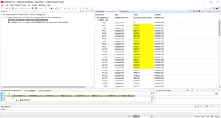
我根据您的提示更新了 Projekt。 请在下面找到带有 main()函数的更新文件。 不幸的是、正如您在下面的图片中看到的、我仍然遇到执行时间问题。 我将周期时间记录到名为 cyclesTemp 的数组中。 您可以看到、周期时间从较高的周期通量开始、然后下降到一个 smaler 周期时间、然后以较高的周期时间再次开始、再下降到 smaler 周期时间。 这种行为似乎是循环的。 main()函数中是否有任何原因导致此行为? 我还发现、在 DMA 控制 pakets 的实际配置中、RXDATA 缓冲区中的数据与 TXDATA 缓冲区不匹配。 370行中的编码检查失败。
测试您的 CCS 项目启动后、它不会传输长度为1024字的 TXDATA 缓冲区的整个内容。 将其更新为将1024字的整个长度 Leeds 传输到上述相同的问题。 您能否扩展项目以传输 TXDATA 缓冲器的整个长度并测量周期时间?
/* USER CODE BEGIN (0) */
/* USER CODE END */

/* Include Files */

#include "HL_sys_common.h"

/* USER CODE BEGIN (1) */
#include "HL_mibspi.h"
#include "HL_sys_dma.h"
#include "HL_het.h"
#include "HL_reg_het.h"
#include "HL_sys_pmu.h"

/* example data Pattern configuration */
#define D_SIZE      128
#define BUFFER_SIZE 1024

void loadDataPattern(uint32 psize, uint16* pptr);
void mibspiEnableInternalLoopback(mibspiBASE_t *mibspi);
void dmaConfigCtrlPacket(uint32 sadd,uint32 dadd,uint32 dsize);
void mibspiDmaConfig(mibspiBASE_t *mibspi,uint32 channel, uint32 txchannel, uint32 rxchannel);

#pragma SET_DATA_SECTION(".sharedRAM")
uint16 TXDATA[BUFFER_SIZE];         /* transmit buffer in sys ram */
uint16 RXDATA[BUFFER_SIZE]= {0};    /* receive  buffer in sys ram */
uint16 TXDATA2[BUFFER_SIZE];         /* transmit buffer in sys ram */
uint16 RXDATA2[BUFFER_SIZE]= {0};    /* receive  buffer in sys ram */
uint16 TXDATA3[BUFFER_SIZE];         /* transmit buffer in sys ram */
uint16 RXDATA3[BUFFER_SIZE]= {0};    /* receive  buffer in sys ram */
uint16 TXDATA4[BUFFER_SIZE];         /* transmit buffer in sys ram */
uint16 RXDATA4[BUFFER_SIZE]= {0};    /* receive  buffer in sys ram */
#pragma SET_DATA_SECTION()

static g_dmaCTRL g_dmaCTRLPKT1, g_dmaCTRLPKT2;    /* dma control packet configuration stack */

static uint32 cycles, cycles_cal;
static uint32 cyclesTemp[1024];

/* USER CODE END */

/** @fn void main(void)
*   @brief Application main function
*   @note This function is empty by default.
*
*   This function is called after startup.
*   The user can use this function to implement the application.
*/

/* USER CODE BEGIN (2) */
/* USER CODE END */

void main(void)
{
/* USER CODE BEGIN (3) */

   uint32 i;
   uint32 j;
   uint32 m;

   _pmuInit_();

   /* - creating a data chunk in system ram to start with ... */
   loadDataPattern(BUFFER_SIZE,&TXDATA[0]);
   loadDataPattern(BUFFER_SIZE,&TXDATA2[0]);
   loadDataPattern(BUFFER_SIZE,&TXDATA3[0]);
   loadDataPattern(BUFFER_SIZE,&TXDATA4[0]);

   clearDataPattern(BUFFER_SIZE,&RXDATA[0]);
   clearDataPattern(BUFFER_SIZE,&RXDATA2[0]);
   clearDataPattern(BUFFER_SIZE,&RXDATA3[0]);
   clearDataPattern(BUFFER_SIZE,&RXDATA4[0]);

   //hetInit();
   //pwmSetDuty(hetRAM1, 0, 1);

   /* - initializing mibspi - enabling tg 0 , length 127 (halcogen file)*/
   mibspiInit();

   /* - enabling loopback ( this is to emulate data transfer without external wires */
   mibspiEnableInternalLoopback(mibspiREG1);
   mibspiEnableInternalLoopback(mibspiREG2);
   mibspiEnableInternalLoopback(mibspiREG3);
   mibspiEnableInternalLoopback(mibspiREG4);

   /* - configuring dma control packets   */
   g_dmaCTRLPKT1.SADD      = (uint32)TXDATA;    /* source address             */
   g_dmaCTRLPKT1.DADD      = (uint32)&(mibspiRAM1->tx[0].data);    /* destination  address       */
   g_dmaCTRLPKT1.CHCTRL    = 0;                 /* channel control            */
   g_dmaCTRLPKT1.FRCNT	   = 8;//1;                 /* frame count                */
   g_dmaCTRLPKT1.ELCNT     = D_SIZE;//32;//D_SIZE;            /* element count              */
   g_dmaCTRLPKT1.ELDOFFSET = 4;                 /* element destination offset */
   g_dmaCTRLPKT1.ELSOFFSET = 0;		            /* element destination offset */
   g_dmaCTRLPKT1.FRDOFFSET = 0;		            /* frame destination offset   */
   g_dmaCTRLPKT1.FRSOFFSET = 0;                 /* frame destination offset   */
   g_dmaCTRLPKT1.PORTASGN  = PORTA_READ_PORTB_WRITE;
   g_dmaCTRLPKT1.RDSIZE    = ACCESS_16_BIT;//ACCESS_64_BIT;	    /* read size                  */
   g_dmaCTRLPKT1.WRSIZE    = ACCESS_16_BIT; 	/* write size                 */
   g_dmaCTRLPKT1.TTYPE     = FRAME_TRANSFER ;   /* transfer type              */
   g_dmaCTRLPKT1.ADDMODERD = ADDR_INC1;         /* address mode read          */
   g_dmaCTRLPKT1.ADDMODEWR = ADDR_OFFSET;       /* address mode write         */
   g_dmaCTRLPKT1.AUTOINIT  = AUTOINIT_ON;       /* autoinit                   */

   g_dmaCTRLPKT2.SADD      = (uint32)&(mibspiRAM1->rx[0].data);    /* source address             */
   g_dmaCTRLPKT2.DADD      = (uint32)RXDATA;    /* destination  address       */
   g_dmaCTRLPKT2.CHCTRL    = 0;                 /* channel control            */
   g_dmaCTRLPKT2.FRCNT	   = 8;//1;                 /* frame count                */
   g_dmaCTRLPKT2.ELCNT     = D_SIZE;             /* element count              */
   g_dmaCTRLPKT2.ELDOFFSET = 0;                 /* element destination offset */
   g_dmaCTRLPKT2.ELSOFFSET = 4;		            /* element destination offset */
   g_dmaCTRLPKT2.FRDOFFSET = 0;		            /* frame destination offset   */
   g_dmaCTRLPKT2.FRSOFFSET = 0;                 /* frame destination offset   */
   g_dmaCTRLPKT2.PORTASGN  = PORTB_READ_PORTA_WRITE;
   g_dmaCTRLPKT2.RDSIZE    = ACCESS_16_BIT;	    /* read size                  */
   g_dmaCTRLPKT2.WRSIZE    = ACCESS_16_BIT;//ACCESS_64_BIT; 	/* write size                 */
   g_dmaCTRLPKT2.TTYPE     = FRAME_TRANSFER ;   /* transfer type              */
   g_dmaCTRLPKT2.ADDMODERD = ADDR_OFFSET;         /* address mode read          */
   g_dmaCTRLPKT2.ADDMODEWR = ADDR_INC1;       /* address mode write         */
   g_dmaCTRLPKT2.AUTOINIT  = AUTOINIT_ON;       /* autoinit                   */

   /* upto 32 control packets are supported. */

   /* - setting dma control packets */
   dmaSetCtrlPacket(DMA_CH0,g_dmaCTRLPKT2);
   dmaSetCtrlPacket(DMA_CH1,g_dmaCTRLPKT1);

   /* - setting the dma channel to trigger on h/w request */
   dmaSetChEnable(DMA_CH0, DMA_HW);
   dmaSetChEnable(DMA_CH1, DMA_HW);

   /* - configuring dma control packets   */
   g_dmaCTRLPKT1.SADD      = (uint32)TXDATA2;    /* source address             */
   g_dmaCTRLPKT1.DADD      = (uint32)&(mibspiRAM2->tx[0].data);    /* destination  address       */
   g_dmaCTRLPKT1.CHCTRL    = 0;                 /* channel control            */
   g_dmaCTRLPKT1.FRCNT     = 8;//1;                 /* frame count                */
   g_dmaCTRLPKT1.ELCNT     = D_SIZE;//32;//D_SIZE;            /* element count              */
   g_dmaCTRLPKT1.ELDOFFSET = 4;                 /* element destination offset */
   g_dmaCTRLPKT1.ELSOFFSET = 0;                 /* element destination offset */
   g_dmaCTRLPKT1.FRDOFFSET = 0;                 /* frame destination offset   */
   g_dmaCTRLPKT1.FRSOFFSET = 0;                 /* frame destination offset   */
   g_dmaCTRLPKT1.PORTASGN  = PORTA_READ_PORTB_WRITE;
   g_dmaCTRLPKT1.RDSIZE    = ACCESS_16_BIT;//ACCESS_64_BIT;     /* read size                  */
   g_dmaCTRLPKT1.WRSIZE    = ACCESS_16_BIT;     /* write size                 */
   g_dmaCTRLPKT1.TTYPE     = FRAME_TRANSFER ;   /* transfer type              */
   g_dmaCTRLPKT1.ADDMODERD = ADDR_INC1;         /* address mode read          */
   g_dmaCTRLPKT1.ADDMODEWR = ADDR_OFFSET;       /* address mode write         */
   g_dmaCTRLPKT1.AUTOINIT  = AUTOINIT_ON;       /* autoinit                   */

   g_dmaCTRLPKT2.SADD      = (uint32)&(mibspiRAM2->rx[0].data);    /* source address             */
   g_dmaCTRLPKT2.DADD      = (uint32)RXDATA2;    /* destination  address       */
   g_dmaCTRLPKT2.CHCTRL    = 0;                 /* channel control            */
   g_dmaCTRLPKT2.FRCNT     = 8;//1;                 /* frame count                */
   g_dmaCTRLPKT2.ELCNT     = D_SIZE;             /* element count              */
   g_dmaCTRLPKT2.ELDOFFSET = 0;                 /* element destination offset */
   g_dmaCTRLPKT2.ELSOFFSET = 4;                 /* element destination offset */
   g_dmaCTRLPKT2.FRDOFFSET = 0;                 /* frame destination offset   */
   g_dmaCTRLPKT2.FRSOFFSET = 0;                 /* frame destination offset   */
   g_dmaCTRLPKT2.PORTASGN  = PORTB_READ_PORTA_WRITE;
   g_dmaCTRLPKT2.RDSIZE    = ACCESS_16_BIT;     /* read size                  */
   g_dmaCTRLPKT2.WRSIZE    = ACCESS_16_BIT;//ACCESS_64_BIT;     /* write size                 */
   g_dmaCTRLPKT2.TTYPE     = FRAME_TRANSFER ;   /* transfer type              */
   g_dmaCTRLPKT2.ADDMODERD = ADDR_OFFSET;         /* address mode read          */
   g_dmaCTRLPKT2.ADDMODEWR = ADDR_INC1;       /* address mode write         */
   g_dmaCTRLPKT2.AUTOINIT  = AUTOINIT_ON;       /* autoinit                   */

   /* upto 32 control packets are supported. */

   /* - setting dma control packets */
   dmaSetCtrlPacket(DMA_CH2,g_dmaCTRLPKT2);
   dmaSetCtrlPacket(DMA_CH3,g_dmaCTRLPKT1);

   /* - setting the dma channel to trigger on h/w request */
   dmaSetChEnable(DMA_CH2, DMA_HW);
   dmaSetChEnable(DMA_CH3, DMA_HW);

   /* - configuring dma control packets   */
   g_dmaCTRLPKT1.SADD      = (uint32)TXDATA3;    /* source address             */
   g_dmaCTRLPKT1.DADD      = (uint32)&(mibspiRAM3->tx[0].data);    /* destination  address       */
   g_dmaCTRLPKT1.CHCTRL    = 0;                 /* channel control            */
   g_dmaCTRLPKT1.FRCNT     = 8;//1;                 /* frame count                */
   g_dmaCTRLPKT1.ELCNT     = D_SIZE;//32;//D_SIZE;            /* element count              */
   g_dmaCTRLPKT1.ELDOFFSET = 4;                 /* element destination offset */
   g_dmaCTRLPKT1.ELSOFFSET = 0;                 /* element destination offset */
   g_dmaCTRLPKT1.FRDOFFSET = 0;                 /* frame destination offset   */
   g_dmaCTRLPKT1.FRSOFFSET = 0;                 /* frame destination offset   */
   g_dmaCTRLPKT1.PORTASGN  = PORTA_READ_PORTB_WRITE;
   g_dmaCTRLPKT1.RDSIZE    = ACCESS_16_BIT;//ACCESS_64_BIT;     /* read size                  */
   g_dmaCTRLPKT1.WRSIZE    = ACCESS_16_BIT;     /* write size                 */
   g_dmaCTRLPKT1.TTYPE     = FRAME_TRANSFER ;   /* transfer type              */
   g_dmaCTRLPKT1.ADDMODERD = ADDR_INC1;         /* address mode read          */
   g_dmaCTRLPKT1.ADDMODEWR = ADDR_OFFSET;       /* address mode write         */
   g_dmaCTRLPKT1.AUTOINIT  = AUTOINIT_ON;       /* autoinit                   */

   g_dmaCTRLPKT2.SADD      = (uint32)&(mibspiRAM3->rx[0].data);    /* source address             */
   g_dmaCTRLPKT2.DADD      = (uint32)RXDATA3;    /* destination  address       */
   g_dmaCTRLPKT2.CHCTRL    = 0;                 /* channel control            */
   g_dmaCTRLPKT2.FRCNT     = 8;//1;                 /* frame count                */
   g_dmaCTRLPKT2.ELCNT     = D_SIZE;             /* element count              */
   g_dmaCTRLPKT2.ELDOFFSET = 0;                 /* element destination offset */
   g_dmaCTRLPKT2.ELSOFFSET = 4;                 /* element destination offset */
   g_dmaCTRLPKT2.FRDOFFSET = 0;                 /* frame destination offset   */
   g_dmaCTRLPKT2.FRSOFFSET = 0;                 /* frame destination offset   */
   g_dmaCTRLPKT2.PORTASGN  = PORTB_READ_PORTA_WRITE;
   g_dmaCTRLPKT2.RDSIZE    = ACCESS_16_BIT;     /* read size                  */
   g_dmaCTRLPKT2.WRSIZE    = ACCESS_16_BIT;//ACCESS_64_BIT;     /* write size                 */
   g_dmaCTRLPKT2.TTYPE     = FRAME_TRANSFER ;   /* transfer type              */
   g_dmaCTRLPKT2.ADDMODERD = ADDR_OFFSET;         /* address mode read          */
   g_dmaCTRLPKT2.ADDMODEWR = ADDR_INC1;       /* address mode write         */
   g_dmaCTRLPKT2.AUTOINIT  = AUTOINIT_ON;       /* autoinit                   */

   /* upto 32 control packets are supported. */

   /* - setting dma control packets */
   dmaSetCtrlPacket(DMA_CH4,g_dmaCTRLPKT2);
   dmaSetCtrlPacket(DMA_CH5,g_dmaCTRLPKT1);

   dmaReqAssign(DMA_CH4, DMA_REQ14);
   dmaReqAssign(DMA_CH5, DMA_REQ15);

   /* - setting the dma channel to trigger on h/w request */
   dmaSetChEnable(DMA_CH4, DMA_HW);
   dmaSetChEnable(DMA_CH5, DMA_HW);

   /* - configuring dma control packets   */
   g_dmaCTRLPKT1.SADD      = (uint32)TXDATA4;    /* source address             */
   g_dmaCTRLPKT1.DADD      = (uint32)&(mibspiRAM4->tx[0].data);    /* destination  address       */
   g_dmaCTRLPKT1.CHCTRL    = 0;                 /* channel control            */
   g_dmaCTRLPKT1.FRCNT     = 8;//1;                 /* frame count                */
   g_dmaCTRLPKT1.ELCNT     = D_SIZE;//32;//D_SIZE;            /* element count              */
   g_dmaCTRLPKT1.ELDOFFSET = 4;                 /* element destination offset */
   g_dmaCTRLPKT1.ELSOFFSET = 0;                 /* element destination offset */
   g_dmaCTRLPKT1.FRDOFFSET = 0;                 /* frame destination offset   */
   g_dmaCTRLPKT1.FRSOFFSET = 0;                 /* frame destination offset   */
   g_dmaCTRLPKT1.PORTASGN  = PORTA_READ_PORTB_WRITE;
   g_dmaCTRLPKT1.RDSIZE    = ACCESS_16_BIT;//ACCESS_64_BIT;     /* read size                  */
   g_dmaCTRLPKT1.WRSIZE    = ACCESS_16_BIT;     /* write size                 */
   g_dmaCTRLPKT1.TTYPE     = FRAME_TRANSFER ;   /* transfer type              */
   g_dmaCTRLPKT1.ADDMODERD = ADDR_INC1;         /* address mode read          */
   g_dmaCTRLPKT1.ADDMODEWR = ADDR_OFFSET;       /* address mode write         */
   g_dmaCTRLPKT1.AUTOINIT  = AUTOINIT_ON;       /* autoinit                   */

   g_dmaCTRLPKT2.SADD      = (uint32)&(mibspiRAM4->rx[0].data);    /* source address             */
   g_dmaCTRLPKT2.DADD      = (uint32)RXDATA4;    /* destination  address       */
   g_dmaCTRLPKT2.CHCTRL    = 0;                 /* channel control            */
   g_dmaCTRLPKT2.FRCNT     = 8;//1;                 /* frame count                */
   g_dmaCTRLPKT2.ELCNT     = D_SIZE;             /* element count              */
   g_dmaCTRLPKT2.ELDOFFSET = 0;                 /* element destination offset */
   g_dmaCTRLPKT2.ELSOFFSET = 4;                 /* element destination offset */
   g_dmaCTRLPKT2.FRDOFFSET = 0;                 /* frame destination offset   */
   g_dmaCTRLPKT2.FRSOFFSET = 0;                 /* frame destination offset   */
   g_dmaCTRLPKT2.PORTASGN  = PORTB_READ_PORTA_WRITE;
   g_dmaCTRLPKT2.RDSIZE    = ACCESS_16_BIT;     /* read size                  */
   g_dmaCTRLPKT2.WRSIZE    = ACCESS_16_BIT;//ACCESS_64_BIT;     /* write size                 */
   g_dmaCTRLPKT2.TTYPE     = FRAME_TRANSFER ;   /* transfer type              */
   g_dmaCTRLPKT2.ADDMODERD = ADDR_OFFSET;         /* address mode read          */
   g_dmaCTRLPKT2.ADDMODEWR = ADDR_INC1;       /* address mode write         */
   g_dmaCTRLPKT2.AUTOINIT  = AUTOINIT_ON;       /* autoinit                   */

   /* upto 32 control packets are supported. */

   /* - setting dma control packets */
   dmaSetCtrlPacket(DMA_CH6,g_dmaCTRLPKT2);
   dmaSetCtrlPacket(DMA_CH7,g_dmaCTRLPKT1);

   dmaReqAssign(DMA_CH6, DMA_REQ24);
   dmaReqAssign(DMA_CH7, DMA_REQ25);

   /* - setting the dma channel to trigger on h/w request */
   dmaSetChEnable(DMA_CH6, DMA_HW);
   dmaSetChEnable(DMA_CH7, DMA_HW);

   //dmaReqAssign(DMA_CH0, DMA_REQ0);
   //dmaReqAssign(DMA_CH1, DMA_REQ1);

   /* - configuring the mibspi dma , channel 0 , tx line -0 , rxline -1     */
   /* - refer to the device data sheet dma request source for mibspi tx/rx  */
   mibspiDmaConfig(mibspiREG1,0,0,1);
   mibspiDmaConfig(mibspiREG2,0,0,1);
   mibspiDmaConfig(mibspiREG3,0,0,1);
   mibspiDmaConfig(mibspiREG4,0,0,1);

//   dmaSetPriority(DMA_CH4, HIGHPRIORITY);
//   dmaSetPriority(DMA_CH5, HIGHPRIORITY);
//   dmaSetPriority(DMA_CH6, HIGHPRIORITY);
//   dmaSetPriority(DMA_CH7, HIGHPRIORITY);
//   dmaSetPriority(DMA_CH0, LOWPRIORITY);
//   dmaSetPriority(DMA_CH1, LOWPRIORITY);
//   dmaSetPriority(DMA_CH2, LOWPRIORITY);
//   dmaSetPriority(DMA_CH3, LOWPRIORITY);

   dmaEnable();
   hetInit();
   pwmSetDuty(hetRAM1, 0, 1);

   i = 0;

while(1)
{
   i++;

   /*Reset Cycle Counter */
   _pmuResetCounters_();
   /*Start Cycle Counter */
   _pmuStartCounters_(pmuCYCLE_COUNTER);
   /*Stop Cycle Counter */
   _pmuStopCounters_(pmuCYCLE_COUNTER);
   /* read the CNNT cycle for calibration */
   cycles_cal = _pmuGetCycleCount_();

   _pmuResetCounters_();

   /*Start Cycle Counter */
   _pmuStartCounters_(pmuCYCLE_COUNTER);

   pwmSetDuty(hetRAM1, 0, 100);

   /* - start the mibspi transfer tg 0 */
   mibspiTransfer(mibspiREG1,0 );

   while(dmaGetInterruptStatus(DMA_CH0, HBC) == FALSE);

   mibspiTransfer(mibspiREG2,0 );

   while(dmaGetInterruptStatus(DMA_CH2, HBC) == FALSE);

   mibspiTransfer(mibspiREG3,0 );

   while(dmaGetInterruptStatus(DMA_CH4, HBC) == FALSE);

   mibspiTransfer(mibspiREG4,0 );

   while(dmaGetInterruptStatus(DMA_CH6, BTC) == FALSE);

   //while(dmaGetInterruptStatus(DMA_CH6, BTC) == FALSE);
   //while(dmaGetInterruptStatus(DMA_CH0, BTC) == FALSE);
   //while(dmaGetInterruptStatus(DMA_CH2, BTC) == FALSE);
   //while(dmaGetInterruptStatus(DMA_CH4, BTC) == FALSE);

   /*Stop Cycle Counter */
   _pmuStopCounters_(pmuCYCLE_COUNTER);
   /* read the CNNT cycle */
   cycles = _pmuGetCycleCount_();
   /*corrected cyles */
   cycles = cycles - cycles_cal;

   if(i < 1024)
   {
      cyclesTemp[i] = cycles;
   }

   pwmSetDuty(hetRAM1, 0, 1);

   mibspiDisableTransfer(mibspiREG1,0);
   mibspiDisableTransfer(mibspiREG2,0);
   mibspiDisableTransfer(mibspiREG3,0);
   mibspiDisableTransfer(mibspiREG4,0);

   dmaREG->BTCFLAG = 0xFFFFFFFF;
   dmaREG->HBCFLAG = 0xFFFFFFFF;

   dmaDisable();

   mibspiDmaConfig(mibspiREG1,0,0,1);
   mibspiDmaConfig(mibspiREG2,0,0,1);
   mibspiDmaConfig(mibspiREG3,0,0,1);
   mibspiDmaConfig(mibspiREG4,0,0,1);

   m = 0x00000000;

   for(j = 0; j < BUFFER_SIZE; j++)
   {
       if((TXDATA[j] != RXDATA[j]) || (TXDATA2[j] != RXDATA2[j]) || (TXDATA3[j] != RXDATA3[j]) || (TXDATA4[j] != RXDATA4[j]))
       {
          m = 0xFFFFFFFF;
       }
   }

   clearDataPattern(BUFFER_SIZE,&RXDATA[0]);
   clearDataPattern(BUFFER_SIZE,&RXDATA2[0]);
   clearDataPattern(BUFFER_SIZE,&RXDATA3[0]);
   clearDataPattern(BUFFER_SIZE,&RXDATA4[0]);

   dmaEnable();
}
   pwmStop(hetRAM1, 0);

   while(1); /* loop forever */

/* USER CODE END */
}

/* USER CODE BEGIN (4) */
/** void mibspiEnableLoopback(mibspiBASE_t *mibspi )
*
*   enabling internal loopback on mibspix
*/
void mibspiEnableInternalLoopback(mibspiBASE_t *mibspi )
{
	/* enabling internal loopback */
    mibspi->GCR1 |= 1U << 16U;
}

void mibspiDisableTransfer(mibspiBASE_t * mibspi, uint32_t group)
{
   mibspi->TGCTRL[group] = (mibspi->TGCTRL[group] & 0x7FFFFFFFU);
}

/** void mibspiDmaConfig(mibspiBASE_t *mibspi,uint32 channel, uint32 txchannel, uint32 rxchannel)
*
*   configuring mibspi dma with
*
*       channel   > mibspi dma channel number
*       txchannel > transmit channel dedicated for mibspi
*       rxchannel > receive  channel dedicated for mibspi
*/
void mibspiDmaConfig(mibspiBASE_t *mibspi,uint32 channel, uint32 txchannel, uint32 rxchannel)
{
	uint32 bufid  = D_SIZE - 1;
	uint32 icount = 0;

    /* setting large count */
    mibspi->DMACNTLEN = 0x00000001;

    /*  setting initial count of DMA transfers */
    mibspi->DMACOUNT[channel] = 8 << 16; //BUFFER_SIZE << 16;

	/* setting transmit and receive channels */
	mibspi->DMACTRL[channel] |= (((rxchannel<<4)|txchannel) << 16);

	/* enabling transmit and receive dma */
	mibspi->DMACTRL[channel] |=  0x8000C000;

	/* setting Initial Count of DMA transfers and the buffer utilized for DMA transfer */
	mibspi->DMACTRL[channel] |=  (icount << 8) |(bufid<<24);

}


/** void loadDataPattern(uint32 psize, uint16* pptr)
*
*   loading a randam data chunk into system ram
*
*     pptr  > sys ram address
*     psize > chunkl size
*
*/
void loadDataPattern(uint32 psize, uint16* pptr)
{
	unsigned int i;

	for(i= 0; i < psize; i++)
	{
	    *pptr = i;
	    pptr++;
	}
 }

void clearDataPattern(uint32 psize, uint16* pptr)
{
    unsigned int i;

    for(i= 0; i < psize; i++)
    {
        *pptr = 0;
        pptr++;
    }
}
/* USER CODE END */
您的 HALCoGen 项目中是否启用了 Cortex-R5高速缓存?
在 QJ Wang 的 TMS570LC4357_MibSPI_DMA_Execution Time\TMS570LC4357_MibSPI1&3_DMA.HCG 示例工程中 、缓存被禁用:
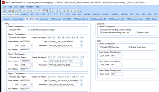
在 MPU 中启用缓存并将 SHAREDRAM 存储器区域标记为可缓存、可能会产生以下影响:
a.读回与 TXDATA 缓冲区不匹配的 RXDATA 缓冲区。 读取 TRM 我还不确定 DMA 是否支持硬件高速缓存一致性。
B.周期时间各不相同。
您好 Raheem、
我将帧计数(F_COUNT)更改为8、以传输具有1024个半字的数据块、我注意到执行时间的差异。
如果 F_COUNT = 1、则传输块块1、块2、...的时间 块10)是相同的。
如果 F_COUNT = 4、则传输时间从块1减少到块4。 块#5的传输时间回到块#1的时间
如果 F_COUNT = 8、则传输时间从块1减少到块8。 块#9的传输时间回到块#1的时间
我不确定导致这种行为的原因、稍后我将做更多的研究和测试。
您好 QJ、
感谢您的回答。 这也正是我观察到的情况。 我很想了解您的发现。 我禁用了高速缓存、因为周期时间仍然不同。
非常感谢你的帮助。


