This thread has been locked.

If you have a related question, please click the "Ask a related question" button in the top right corner. The newly created question will be automatically linked to this question.

mcu掉电存储实现

Other Parts Discussed in Thread: MSP-EXP430FR2311, MSPWARE

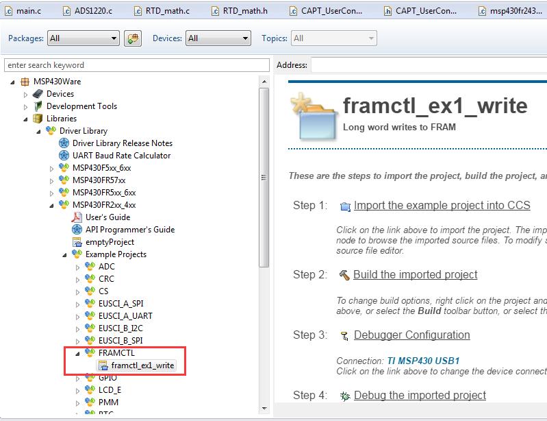
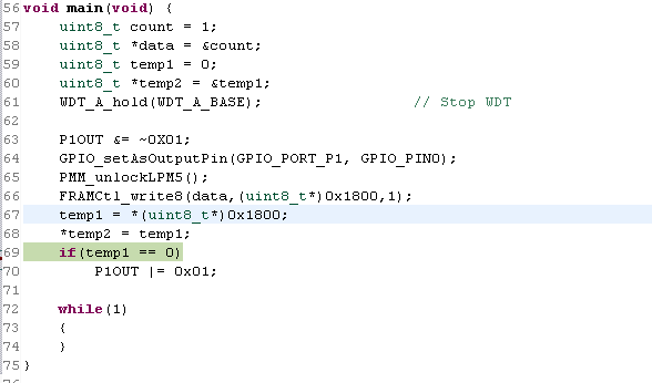
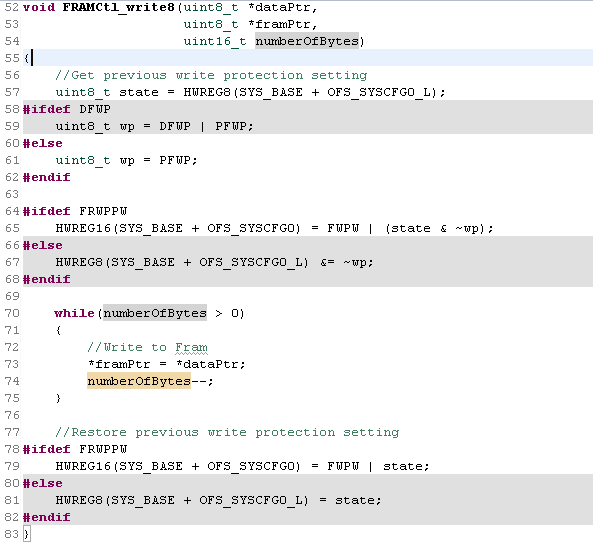
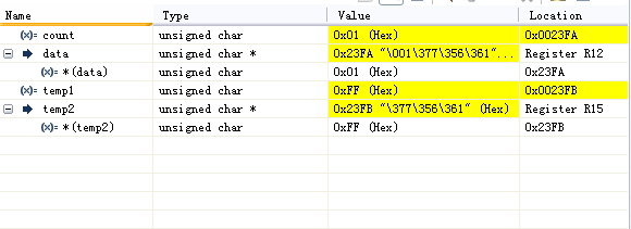
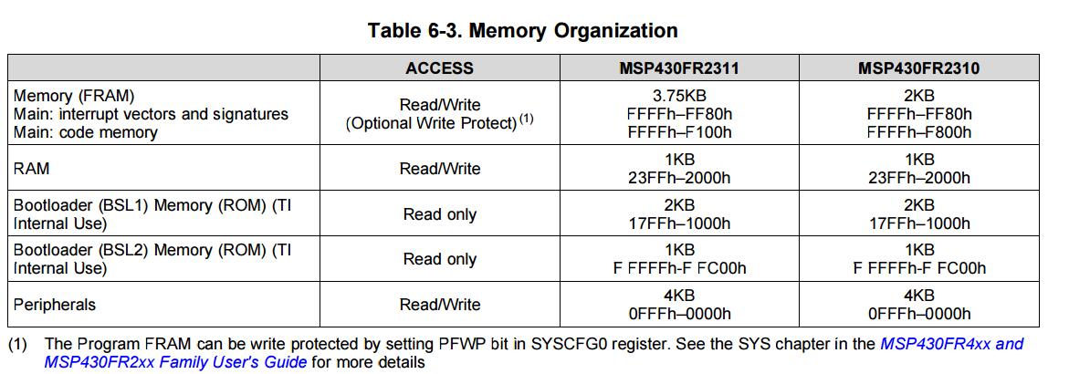
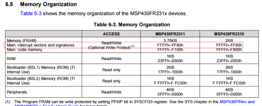
您好,正在用ti的MSP-EXP430FR2311。需要实现程序中某些参数的掉电存储。在driverlib users guide和产品users guide 都没找到相关的内容。不知道是否有对flash进行读写操作的例程或者操作说明。在drivelib example也没找到相关例程。

  • Outman J 说:

    您好,正在用ti的MSP-EXP430FR2311。需要实现程序中某些参数的掉电存储。在driverlib users guide和产��users guide 都没找到相关的内容。不知道是否有对flash进行读写操作的例程或者操作说明。在drivelib example也没找到相关例程。

    FR2311存储技术不是flash,而是 FRAM.

    例程如图,

  • 这个msp430内部是fram,不是flash。如果你的参数不多的话,直接存储在信息存储区就可以,我记得mspware里有相关例程

  • dirtwillfly 说:

    这个msp430内部是fram,不是flash。如果你的参数不多的话,直接存储在信�存储区就可以,我记得mspware里有相关例程

    请指明具体例程。如何存储在信息存储区?

  • 可以直接把变量定义到fram区这样的吗,这样掉电,变量的值也不会丢失。

  • 例程里是FR2433,用的0x1800存储地址。

    /* --COPYRIGHT--,BSD_EX
     * Copyright (c) 2014, Texas Instruments Incorporated
     * All rights reserved.
     *
     * Redistribution and use in source and binary forms, with or without
     * modification, are permitted provided that the following conditions
     * are met:
     *
     * *  Redistributions of source code must retain the above copyright
     *    notice, this list of conditions and the following disclaimer.
     *
     * *  Redistributions in binary form must reproduce the above copyright
     *    notice, this list of conditions and the following disclaimer in the
     *    documentation and/or other materials provided with the distribution.
     *
     * *  Neither the name of Texas Instruments Incorporated nor the names of
     *    its contributors may be used to endorse or promote products derived
     *    from this software without specific prior written permission.
     *
     * THIS SOFTWARE IS PROVIDED BY THE COPYRIGHT HOLDERS AND CONTRIBUTORS "AS IS"
     * AND ANY EXPRESS OR IMPLIED WARRANTIES, INCLUDING, BUT NOT LIMITED TO,
     * THE IMPLIED WARRANTIES OF MERCHANTABILITY AND FITNESS FOR A PARTICULAR
     * PURPOSE ARE DISCLAIMED. IN NO EVENT SHALL THE COPYRIGHT OWNER OR
     * CONTRIBUTORS BE LIABLE FOR ANY DIRECT, INDIRECT, INCIDENTAL, SPECIAL,
     * EXEMPLARY, OR CONSEQUENTIAL DAMAGES (INCLUDING, BUT NOT LIMITED TO,
     * PROCUREMENT OF SUBSTITUTE GOODS OR SERVICES; LOSS OF USE, DATA, OR PROFITS;
     * OR BUSINESS INTERRUPTION) HOWEVER CAUSED AND ON ANY THEORY OF LIABILITY,
     * WHETHER IN CONTRACT, STRICT LIABILITY, OR TORT (INCLUDING NEGLIGENCE OR
     * OTHERWISE) ARISING IN ANY WAY OUT OF THE USE OF THIS SOFTWARE,
     * EVEN IF ADVISED OF THE POSSIBILITY OF SUCH DAMAGE.
     *
     *******************************************************************************
     *
     *                       MSP430 CODE EXAMPLE DISCLAIMER
     *
     * MSP430 code examples are self-contained low-level programs that typically
     * demonstrate a single peripheral function or device feature in a highly
     * concise manner. For this the code may rely on the device's power-on default
     * register values and settings such as the clock configuration and care must
     * be taken when combining code from several examples to avoid potential side
     * effects. Also see www.ti.com/grace for a GUI- and www.ti.com/msp430ware
     * for an API functional library-approach to peripheral configuration.
     *
     * --/COPYRIGHT--*/
    //******************************************************************************
    //   MSP430FR243x Demo - Long word writes to FRAM
    //
    //   Description: Use long word write to write to 512 byte blocks of FRAM.
    //   Toggle LED after every 100 writes.
    //   NOTE: Running this example for extended periods will impact the FRAM
    //   endurance.
    //   ACLK = REFO, MCLK = SMCLK = default DCODIV = ~1MHz
    //
    //   It is recommended to disable interrupt while code is writing to main FRAM,
    //   because it is dangerous for running the interrupt services routine with 
    //   PFWP disabled.
    //   This code examples is using DFWP which wouldn't have dangerous. But it is 
    //   recommended to disable interrupt if user is using PFWP.
    //
    //           MSP430FR2433
    //         ---------------
    //     /|\|               |
    //      | |               |
    //      --|RST            |
    //        |               |
    //        |          P1.0 |---> LED
    //
    //   Ling Zhu
    //   Texas Instruments Inc.
    //   Feb 2015
    //   Built with IAR Embedded Workbench v6.20 & Code Composer Studio v6.0.1
    //******************************************************************************
    #include <msp430.h>
    
    void FRAMWrite(void);
    
    unsigned char count = 0;
    unsigned long *FRAM_write_ptr;
    unsigned long data;
    
    #define FRAM_TEST_START 0x1800
    
    
    int main(void)
    {
        WDTCTL = WDTPW | WDTHOLD;               // Stop watchdog timer
    
        P1OUT &= ~BIT0;                         // Clear P1.0 output latch for a defined power-on state
        P1DIR |= BIT0;                          // Set P1.0 to output directionOUT
    
        PM5CTL0 &= ~LOCKLPM5;                   // Disable the GPIO power-on default high-impedance mode
                                                // to activate previously configured port settings
        data = 0x11111111;                      // Initialize dummy data
    
        while(1)
        {
            data += 0x00010001;
            FRAM_write_ptr = (unsigned long *)FRAM_TEST_START;
            FRAMWrite();
            count++;
            if (count > 100)
            {
                P1OUT ^= 0x01;                  // Toggle LED to show 512 bytes
                count = 0;                      // have been written
                data = 0x11111111;
            }
        }
    }
    
    void FRAMWrite (void)
    {
        unsigned int i=0;
    
        SYSCFG0 = FRWPPW | PFWP;
        for (i = 0; i < 128; i++)
        {
            *FRAM_write_ptr++ = data;
        }
        SYSCFG0 = FRWPPW | PFWP | DFWP;
    }
    
  • 这样mcu上电后,就可以通过这个地址读取到我之前存的数据了对的吧 ?(*FRAM_TEST_START )

  • 谢谢回复,在库中找到了 相应的例程。那该怎么去读取fram中已知地址的值呢。(关机前将数据存进了0x1800,上电后该怎么去获取这个值呢?)

  • FRAMWrite_Char((uint8_t *)0x1800, 0xAA);
    uint8 temp;
        temp = *((uint8_t *)0x1800);

     写函数 每个芯片可能有所差异,以下为范例
    void FRAMWrite_Char(uint8_t *FRAM_write_ptr, uint8_t data)
    {
        SYSCFG0 = FRWPPW | PFWP;
        *FRAM_write_ptr = data;
        SYSCFG0 = FRWPPW | PFWP | DFWP;
    }

     
  • 您好 用这样的方式我并没有正确读到保存下来的数据。贴上代码如图

    保存值为 0x01 获取值为0xff

  • 你用的哪颗芯片?

  • Outman J 说:

    MSP-EXP430FR2311

    2311 没有 info memory。你可以存到程序FRAM 里面。

  • 这样说数据存在地址0FF80h-0FFFFh是可以的吧? 那直接地址赋值会不会被程序给覆盖或者改写掉程序的内容?应该在哪一段地址进行保存呢?

  • 谢谢你的答复 确实那一块地址是可以正确操作的,那和程序的存储会不会存在冲突,该怎么去避免呢?

  • Outman J 说:

    谢谢你的答复 确实那一块地址是可以正确操作的,那和程序的存储会不会存在冲突,该怎么去避免呢?

    先看一下现有的程序占多大的空间,然后用户数据从另一端开始存。

  • 刚刚在试着往两端的地址进行读写操作,然后有有关于地址0xFFF1的报错,修改程序后再连接开发板显示,

    Error connecting to the target:
    The Debug Interface to the device has been secured

    是因为和调试模块相关的代码地址内容被重写了么?现在该怎么恢复?

  • Outman J 说:

    刚刚在试着往两端的地址进行读写操作,然后有有关于地址0xFFF1的报错,修改程序后再连接开发板显示,

    Error connecting to the target:
    The Debug Interface to the device has been secured

    是因为和调试模块相关的代码地址内容被重写了么?现在该怎么恢复?

    FFFFh - FF80h 不要去写。

  • Outman J 说:

    刚刚在试着往两端的地址进行读写操作,然后有有关于地址0xFFF1的报错,修改程序后再连接开发板显示,

    Error connecting to the target:
    The Debug Interface to the device has been secured

    是因为和调试模块相关的代码地址内容被重写了么?现在该怎么恢复?

    你应该是写了 JTAG 的 signature 把片子锁住了。需要用 BSL 解锁。

  • 没有其他方式了吗? 还没了解过BSL方式编码,能给我详细的说明或者文档么,我有找到MSP430FR4xx and MSP430FR2xx Bootloader (BSL) users guide 

    还有其他资料和说明么?

  • Outman J 说:

    没有其他方式了吗? 还没了解过BSL方式编码,能给我详细的说明或者文档么,我有找到MSP430FR4xx and MSP430FR2xx Bootloader (BSL) users guide 

    还有其他资料和说明么?

    需要BSL 工具的。

    现在最简单的办法,申请新片子换上去。

  • 您好,只能换了个430的样片。那FRAM区域里F100h到FFFFh是代码存储区域,其中FF80h到FFFFh是存储中断向量和标志位的地方,这样的么?

    所以不对那部分区域进行操作就不会有问题了对吧? 另外在F100h到FFFFh是代码存储区域,烧写的代码是从高位到低位填还是低位到高位填应该怎么获知?

    这样才好确定掉电存储的参数是从F100h开始写入还是从FFFFh开始写入,以避免对代码段存储空间的错误操作。不知这样的理解对否。

    感谢您的解答!

  • Outman J 说:

    您好,只能换了个430的样片。那FRAM区域里F100h到FFFFh是代码存储区域,其中FF80h到FFFFh是存储中断向量和标志位的地方,这样的么?

    所以不对那部分区域进行操作就不会有问题了对吧? 另外在F100h到FFFFh是代码存储区域,烧写的代码是从高位到低位填还是低位到高位填应该怎么获知?

    这样才好确定掉电存储的参数是从F100h开始写入还是从FFFFh开始写入,以避免对代码段存储空间的错误操作。不知这样的理解对否。

    感谢您的解答!

    理解正确。烧写的代码是从高位到低位填还是低位到高位填应该怎么获知?可以在debug的时候,看一下memory地址。